


 Get A Quote
  (224)366-0290
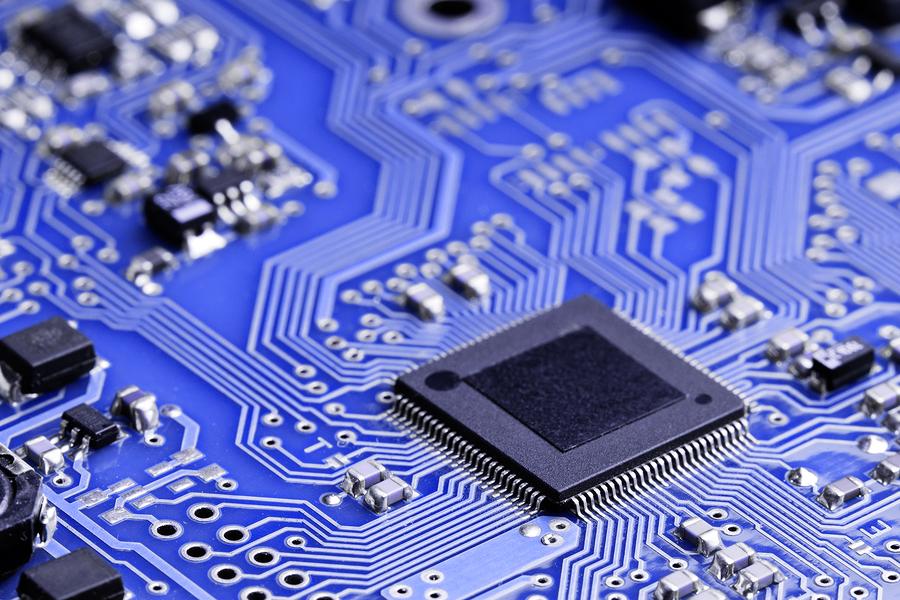
There’s a particular sense of accomplishment that comes with taking on a difficult task. I enjoy tinkering with carving spoons and other utensils in my spare time. They appear easy to create, but the challenge lies in getting the curvature exactly right, smoothing out the wood, and applying whatever cosmetic treatments you choose to the handle.
Whenever it comes to the production process after PCB design, you might be one of the handfuls who has tackled the problem of inserting vias into your design. While you would quickly enjoy the advantages of incorporating this innovation into your board’s structure, there would undoubtedly be a few roadblocks to overcome; nonetheless, such is life.
Aspect ratios are extremely important in the construction of an aspect ratio of PCB and must not be overlooked. They could leave you with a torn circuit board that can’t form good connection points for you through plating or even electronic component installation if they’re ignored.
When creating a printed circuit board, numerous capabilities are taken into consideration (PCB). The aspect ratio of PCB is one such capacity. The PCB aspect ratio is the proportion of a PCB’s thicknesses to the diameter of the drilled hole. In the plating procedure, the aspect ratio of PCB is very significant. The ratio indicates the chemical procedure’ capability to produce copper-plated holes. It becomes increasingly difficult to produce accurate plating when the aspect ratio soars.
Examples
Here are some instances of how the aspect ratio of PCB might be used:
- The aspect ratio is 2:1 if the board thickness is 62 mils and the drilled hole diameter is 31 mils.
- The thickness of the PCB is 64 mils, and the width of the drilled hole is eight mils for an 8:1 aspect ratio.
- The board thickness is 80 mils for a 10:1 aspect ratio, while the drilled hole diameter is eight mils.
What is its importance in the PCB industry?
Through-holes and blind/buried vias, which are the soul of the entire PCB layout and the panel points of different layers, are known to be split into plated holes. The more difficult it is for the plating solution to flow through the hole and the harder it is for the center sections of the holes to get uniformly plated in the actual plating process, the thicker the PCB thickness and the smaller the holes are (the low current areas).
As a result, the larger the aspect ratio, the more difficult plating becomes; achieving reliable plating often necessitates more modern equipment, more expensive additives, and better manufacturing procedures. The aspect ratio is important for establishing a uniform plating procedure: the lower the aspect ratio, the more likely the copper plating will be uniform throughout the hole’s length. Aspect ratios greater than a fabricators maximum allowable might lead to inadequate hole plating, resulting in a damaged net in the case of a via hole or assembling failure in the case of a piece plated through-hole.
Fabricators typically list maximum manufacturable aspect ratios for various procedures, including through-holes and micro vias. Of course, every fabricator might release a unique set.
So, how do you know whether it’s true?
The manufacturer will typically verify the aspect ratio as part of the DFM procedure. But here’s the problem: both the designer and the manufacturer are omitting important details:
The board thickness and material (copper and dielectric) thickness values are not included in the Gerber data – as they are not part of the format – and are normally given in the documentation or a drawing. Must provide these data o the manufacturer to verify the via aspect ratio of PCB fully. This is, regrettably, a manual operation that is prone to error.
You, as the designer, might not be aware of your manufacturer’s essential via aspect ratio of PCB capacity, and the resultant ambiguity might lead to additional, resource-intensive design spins. Is it possible to prevent them?
At Absolute PCB, our PCB Aspect Ratios can be seen in the below table
There are key characteristics to bear into consideration when designing aboard, such as the minimum trace width and space and the minimum via size. Another feature to keep in mind is the Aspect Ratio of PCB .
The Aspect Ratio of PCB is the proportion of a PCB’s thickness to the diameter of the tiny hole that has been drilled. The plating procedure becomes increasingly challenging as the aspect ratio increases.
As the aspect ratio rises, more plating is required, and the danger of cracking as a result of expansion amidst the process rises proportionally.
You could select from a variety of PCB thicknesses and hole minimum sizes. The various aspect ratios are available to you:
10:1
Board Thickness Min. Hole Size
Eight mil – 62 mil six mil
80 mil 8 mil
93 mil nine mil
125 mil 12 mil
We are a prominent supplier of printed circuit boards with a wide range of capabilities and specifications. We have over 30 years of expertise, allowing us to service clients in a variety of industries. We offer high-quality PCBs at reasonable pricing. Furthermore, we offer the fastest turnaround times in the business. Please get in touch with us as soon as possible if you have any questions about the various varieties of PCBs we have available.
Customer Service -There is a lot of crucial considerations to examine when selecting a Complete PCB Assembly service provider. Our offerings have been developed to guarantee that we can deliver the very finest in each element of PCB services. We give efficient constructions with quick turnaround times; we follow high North American Quality Management standards for our PCB Assembly in Canada. We deliver a selection of PCB Choices at a Standard Price to help you maintain your costs as low as possible. All of these components of our service represent our commitment to giving our customers the best possible experience. Still, the actual secret to our success is our outstanding team of PCB professionals, who work with you every step of the way to assure your absolute happiness on every project.
DFM Checking is one of our basic Cost-Free PCB Services since our staff is here to assist you with even the tiniest points of your design. We confirm that your design is well suited to our production skills before beginning PCB fabrication, and we offer ideas for enhancing build efficiencies in future versions of the project. We could discover flaws or ambiguity in your PCB Design Files through this careful verification procedure before production begins, possibly saving you time and money on fixing or rebuilding the defective boards.
You may take benefit of our Parts Procurement team if you select our PCB Assembly services, and rest assured that your Bill of Materials (BOM) is in the best possible hands. We can make use of our long-standing relationships with reputable North American component providers to help you save money on parts and avoid delays caused by late shipping. When your parts run out of stock, our purchasing team works directly with you to find replacements, and we can even assist you in locating hard-to-find or obsolete components.
Call to Action
With the Absolute Electronics team on your side, you can expect nothing but the best PCB services—from quality to lead time to overall cost—all delivered with a simple and uncomplicated support system. Please feel free to contact us at any moment to learn more about our PCB services and team! You can contact us via email or toll-free phone.