


 Get A Quote
  (224)366-0290
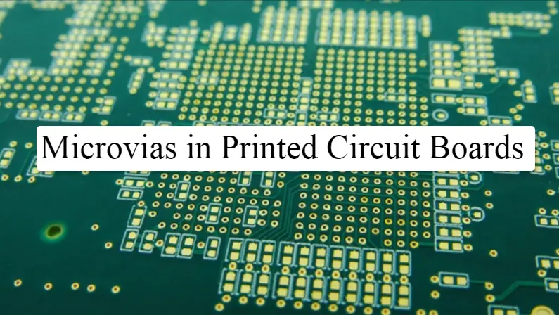
What are the microvias?
With the emerging development of smart technology, different PCBs are getting more common in devices and smart gadgets. Advanced PCBs that consist of multiple layers are suitable options for advanced gadgets containing many features. Different board layers of a multi-layer PCB require to remain interconnected for making the device function. The multiple boards of such a PCB retain uninterrupted interconnection through vias or holes. Microvias are the small micro-holes through which the layers of a multi-layer PCB remain connected. In general, the maximum size of micro is likely to be around 150 microns and not more than that. The diameter of a microvia is way lesser than a PTH of a printed circuit board. The primary purpose of drilling a microvia is to connect a layer of the PCB with another layer. But a microvia can’t connect more than one board layer of a printed circuit board. Usually, engineers use lasers for creating micro vias in the board layers of PCBs, which makes microvias safer options than PTHs. Because there won’t be even a small amount of residue after you drill a microvia using a laser. Drilling a microvias in printed circuit boards is an excellent option for completing the circuit.
Types of microvia in PCB?
If you observe, you will find different kinds of microvias in printed circuit boards. However, all those types of microvias share similar characteristics. Let’s talk about the typical characteristics of the different kinds of microvias.
- Generally, the standard aspect ratio of a microvia is 2:1, and that’s why you cannot connect more than two board layers using a microvia. The aspect ratio of a microvia is unlike a PTH as a PTH possesses a more significant aspect ratio of 10:1.
- The neck region of a microvias in printed circuit boards tends to get injured or fractured pretty quickly if it goes through a constant vibration of a mechanical shock for an extended period.
These are the main characteristics that all kinds of microvias include. You must be aware of these characteristics before you drill a microvia in a circuit. The following types are the most common types of microvias that are found in most PCBs.

Blind microvias
The span of a blind microvia starts from the circuit’s surface layer, and it stretches up to one-two layers under the surface. However, the best application of a blind microvia is when it is used to connect the surface with a single layer underneath. Blind microvias are not much efficient in securing more than one layer under the surface of a PCB.
Buried microvias
In the case of a buried microvia, none of the ends of the microvia touches the surface of the circuit. Like blind microvias, buried microvias also deliver the best durability and performance when applied to connect single layers.
Stacked microvias
Stacked microvias are the best options for interconnecting more than two layers. Stacked microvias are stacks of numerous buried microvias. Sometimes, a blind microvia is also implemented over a buried microvia to create a stacked microvia. When it comes to an HDI PCB, stacked microvias are the best options for different interconnecting layers of the PCB.
Advantages of microvias
- As you know, the diameter of a microvia is way smaller than a PTH or other types of hole; these vias are efficient in saving space in a circuit. While you’re designing a printed circuit board, you have to consider the space factor to make the course more efficient. While bigger vias or PTHs consume a lot of space in the circuit, microvias can interconnect multiple board layers finishing shorter spaces. That’s why microvias can be space-savors for you while designing a printed circuit board.
- The bigger the circuit board you will purchase, the more money you will have to spend. While fitting a lot of components into the circuit board, you find it difficult to manage space. You become bound to buy a bigger circuit to include all the standard components in such a case. To save your money up to some extent, you can use microvias instead of bigger holes. As microvias consume lesser spaces, you won’t have to buy a bigger circuit to fit all the mandatory components into it. This way, you will be able to cut off additional expenses as well.
- While you’re using microvias for connecting different layers of a PCB, you stand lower risks of having manufacturing defects. In most cases, lasers are used to create microvias in printed circuit boards, which’s probably the safest technique for drilling microvias in printed circuit boards.
- As you use microvias in printed circuit boards, you will not have to face difficulties when you initiate the fabrication process. Bigger vias and holes can cause fabrication issues. But in the cases of microvias, you will never have to face such problems.
- When it comes to HDI circuits, microvias significantly impact the integrity of signals in such circuits. In large and high-speed circuits, large vias usually create high amounts of radiation as those function as high radiating antennas. That’s why technicians prefer using microvias in such high-speed circuits as microvias generate lesser amounts of radiation. Due to the smaller sizes of microvias, these function as smaller antennas that emit a limited amount of radiation.
- Microvias usually have trace lengths that are shorter than the trace lengths of PTHs and other big holes. This is because of the shorter diameters and sizes of the microvias.
- If you consider reliability, microvia technology is more innovative and efficient in comparison with through holes. No matter what the size of the PCB is, microvias are way more reliable than through holes or other holes.
- The shorter size of a microvia enhances the RF capability and EMC characteristics of this. In addition to that, the screen resistor’s integration also gets improved if you use microvias in printed circuit boards.
These are the vivid benefits of microvias. All the features and benefits collectively make microvias better options than other bigger holes. Microvias are the best options for improving the quality and functionality of smaller PCBs. Besides that, microvias are also compatible with high-speed and more oversized PCBs. In simple words, microvias are turning the world of PCBs into a better version.
Capabilities of Microvia in PCB
- Microvias are capable of establishing connections between two different board layers of a printed circuit board.
- Via-in-pad microvias are a bit different from regular microvias. The via-in-pad microvias are the microvias that get placed directly on the solar pads. The via-in-pad feature of a microvia plays a significant role in miniaturizing the circuit board. Miniaturizing the circuit board is necessary to maintain the condition and the functions of the circuit board.
- Microvias allow engineers and technicians to design the component layout of circuit boards with smaller BGA pitches. BGA pitches are the factors that you have to keep in mind when creating the component layout of a circuit board. In case of implementing bigger holes, you have to plan bigger PGA pitches in the layout. On the other side, microvias don’t require bigger BGA pitches due to their small sizes.
- It is highly possible to generate high wiring density using microvias. That’s another maximum capability of microvias. If you intend to enhance the wiring density, using microvias is the simplest way to do so. This is also the most cost-efficient way to increase the wiring density of a PCB.
- You will never have a complaint regarding the reliability of microvias. Microvias are great options for maintaining the thermo-mechanical reliability of circuit boards. The performances and functions of PCBs also get impacted by the reliability of microvias.
- Promoting future-oriented technology is another remarkable technology that microvias offer. As mentioned before, microvias consume way fewer spaces in circuit boards. Therefore, microvias allow circuit boards to be smaller and more compact. As technology is proceeding towards maximum improvement, devices and gadgets tend to be smaller than before. The usage of microvias is the leading reason behind this. The circuits of the gadgets are becoming smaller due to the presence of microvias. Hence, it can be claimed that the extended usage of microvias is promoting the future of technology.
- Coping with the inductance and capacitance effects of a circuit is one of the significant troubles a technician has to deal with. Usage of microvias makes it easier to reduce those effects and allows the circuit to perform better. As these effects get controlled by microvias easily, the other components of a circuit perform better. This can also be regarded as one of the impressive capabilities of microvias that are helpful for PCBs.
Key Takeaway:-
In this article, we discussed different aspects of microvias in printed circuit boards, and we hope that these details helped you understand the functions of microvias. If you have further questions about microvias, you can contact us directly to get your question answered. Reach our expert team to get the best solutions regarding microvias.