


 Get A Quote
  (224)366-0290
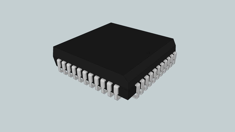
Those who are familiar with the term PCB or printed circuit board must have heard about different electronic component packages that get used for shaping a PCB. Among them, PLCC is one of the lesser-used integrated circuit alternatives that contribute a lot of benefits in the realm of prototype PCB assembly.
If you are interested to know what a PLCC is, an LCC package, several benefits provided by a PLCC packages, and the distinction between a PLCC packages and an LCC package, this guide will help you enormously. So, let’s start reading without wasting any more time.
What are PLCCs?
PLCC refers to a Plastic Leaded Chip Carrier, which is a four-sided ‘J’ leaded surface mount tool. It gets made using materials that are likely to be green in color. It is a configuration of the SMD IC (Integrated Circuit) package that has both possibilities of getting regulars ordered in the circuit board and mounted in the socket. In short, this chip carrier generally facilitates the integrated circuits to get attached to the printed circuit board (PCB) either by soldering or mounting in the socket. Conventionally, the IC or integrated circuit or the chip gets put inside a rectangular or square-shaped PLCC.
When it comes to the pattern of a PLCC, it appears to be either rectangular or square. Both of these PLCCs were invented almost at the same time, where the square was one year older than the other one. Both of these two shapes get used largely in the present day according to the requirements of distinct users. Furthermore, one thing you must keep in mind is whether your picked PLCC dissipates heat or not. Remember, almost all PLCCs look identical. Therefore, you must be aware when it comes to the heat-dissipating ability of a certain PLCC.
Being budget-friendly and profitable at the same time, a PLCC easily works as a substitute for the expensive ceramic leaded chip carriers or CLCC. Additionally, the special ‘J’ shape enables the constructor to solder it or mount it inside the socket without any hassle. On the other hand, if it gets damaged or eradicated, anyone can easily restore it even without replacing the printed circuit board. You can find other wing-shaped chip carriers that are not as compatible as the ‘J’ formed one used in PLCC. These benefits provided by PLCCs have successfully rendered it the number one choice of most users and the most used package in the world of chip carriers.
So, it was, in short, an abstract explanation of PLCCs. For compiling more important details, keep reading.
PLCC packages what is an LCC package?
In the world of electronics, a chip carrier gets counted as an inevitable part of the entire circuit board. It appears in various shapes, sizes, and infrastructures and gets used accordingly. Some of them are ‘J’ shaped (like PLCC), whereas some are gull-wing shaped (like QFP). In the same way, some carriers are leaded (like PLCC), whereas some do not contain any lead. The one that does not contain a lead is called LCC or a Leadless Chip Carrier.
LCC is a relatively newer and evolutionary version of a plastic chip carrier that does not contain any lead like a PLCC chip. It contains a ceramic base that has materialized castellation or pads both on the side and the bottom of the package. It consists of pads on all four sides of the LCC package. Rather than using a lead like a PLCC package, this package encompasses pins either made of metal or ceramic.
Advantages of using PLCC Components packages
As mentioned earlier, PLCC packages contain a handful of benefits that allow them to stand apart from other chip carriers. From the construction of a PLCC packages to its price range, all make it the most familiar and the most used package in the current market. So, let’s look at some benefits of utilizing PLCC components packages.
The ‘J’ shape
If you take your time to analyze a PLCC packages from top to bottom, the first thing you will notice is its shape. Unlike other surface mount devices, a PLCC package always uses a ‘J’ shaped lead that not only makes it unique from other devices but also provides it with a few benefits.
Firstly, being like a big ‘J’, a PLCC is more saves a lot more space compared to other packages. There are so many surface-mount devices that encompass leads like ‘L’ shaped, gull-winged, etc. But, none of them works as efficiently as a ‘J’ shaped PLCC packages can. For instance, a Quad Flat Package containing gull-wing leads always gets folded outwards in the toe of the mounting device, while PLCC leads tend to get folded inside of the SMD.
As a result, if the PLCC packages leads somehow get damaged, you do not have to reopen and reconstruct the entire printed circuit board. All you have to do is to remove the PLCC from the board and insert a new one.
Attaching a PLCC depends on the user
A plastic leaded chip carrier can be attached to a circuit board both by using the traditional soldering or attaching it rapidly to the socket using the mounting technique. This can be different for different devices, depending on the goal.
For example, in case your PLCC contains a PLD chip or programmable logic device chip inside, it would be better to project it solely before attaching it to the circuit board. In this way, you can easily identify the errors (only if there has any) and troubleshoot them. You must keep it in mind before attaching the chip inside, exclusively if you are working with a programmable logic device and a circuit board where no onboard programming is attainable.
Provides safety to the chip
The best part of working with a PLCC packages is that with it, you can get assured about the safety and stability of the chip inside the carrier. With a PLCC, you can handily attach it to the socket. In this way, the chip inside the carrier remains intact and stable instead of getting affected by anything.
On the other hand, if you prefer to blend the PLCC packages inside the circuit board, you do not have to do it instantly. Hence, the chip that is in the carrier will not face any direct heat of soldering and remain safe for a long time.
Cost-effectiveness
When it comes to the price of a PLCC packages, in a word, it is affordable and cost-effective. Where you have to spend lots of money while generating a ceramic leadless chip carrier, it would be better to replace it with the more sustainable and affordable PLCC.
PLCC packages PLCC vs LCC package
An LCC or Leadless Chip Carrier is a newer and arguably one of the best inventions that differ from a PLCC IC package in many places. However, in shape and size, both of them share lots of similarities with each other. Both of them come in rectangular and square shapes. Furthermore, you can get your hands on plastic-made or ceramic-made LCC packages as well.
Now, let’s have a look at the major differences between a PLCC packages and an LCC package.
Leaded vs. Leadless
The fundamental difference between an LCC package and a PLCC IC packages fabricates inside the name of them. While PLCC stands for Plastic Leaded Chip Carrier, LCC means Leadless Chip Carrier. That simply indicates that an LCC carrier does not comprise any lead like a PLCC chip carrier. Rather than using a lead like a PLCC packages, this package encompasses pins and pads either made of metal or ceramic.
Versatility
LCC packages get used more than a PLCC packages. It is because an LCC package is far more portable, convenient, and adaptable. You can effortlessly employ an LCC package when in doubt whether you should mount or unmount the integrated circuit rather than entirely soldering the package into the printed circuit board.
Attachment procedure
As we know, it is possible to both solder a PLCC packages onto the printed circuit board and wields the surface-mount technique for attaching the PLCC chip in the socket. In this case, the user can select whether it will be better to choose the first option or they should pick the mount-surface technique depending on the situation. But, with an LCC package, you can never go for the soldering option as it does not support this one. So, you always have to select the second option, which is the mount-surface technique.
Call to action
Now, when you have compiled almost all essential information about a Plastic Leaded Chip Carrier or PLCC, hopefully, choosing the perfect one for your printed circuit board will no longer be a matter of concern for you. With this package, you get the opportunity to select the best-suited one for your project when it comes to the pattern, size, attaching method, and more. Additionally, you do not have to spend lots of money to get your hands on a reliable and versatile PLCC package.
So, now, it is time for you to contact professional PLCC service providers who have years of experience on the ground. We, as an old player in the field, promise to provide our customers with 100% accurate, safe, sustainable, and the best product in the market. We always prioritize our clients’ requirements and maintain great professionalism. So, if you have any queries regarding PLCC or how does it work, you can contact us to attain our guidance and services at your early convenience.