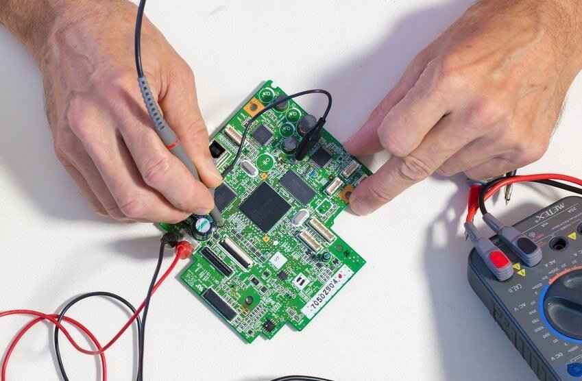
This is how you can design a printed circuit board yourself
Everyone has come across a printed circuit board at least once in their lifetime. We are no strangers to this modern electronic equipment that has spread its legs into every new-age electronic device these days. But seldom do we know about the PCB assembly services and what goes into its production!
A PCB or printed circuit board is a device used to mechanically support and link electronic components via a non-conductive substrate. This is what goes into making a printed circuit board all by yourself, have a look:
- The substrate of the PCB is made up of a thin, non-conductive material which is very hard to bend. It is covered with a thin layer of copper foil to provide electrical connectivity to other parts of the PCB with the help of engraved wiring, leaving the rest of the PCB in a mesh-like small line.
- The above process makes up for the first part of the whole PCB assembly services. The lines of wires carved are different than those from the PCB itself. PCBs are colored either brown or green to make since that is the color of the solder paint which consists of an insulating layer that protects the copper wires and the rest of the parts from being soldered into the incorrect place.
- After the substrate is covered with a thin layer of copper foil and fabricated with a light-drawn wiring, the printed circuit board is ‘printed’ on the metal conductor.
- The next step? Simply, drill and paste the required components but before drilling remember to plate a hole so as the internal layers can be connected to each other.
- While doing all this, be wary of the resin substrate undergoing chemical changes when it is heated. Also, make sure the solder ink is covered so that the light-drawn wires do not touch the rest of the plate.
- Marking the PCB plate is the last step in the process. Each and every component is marked so as to exhibit the exact position of each and every part.
Also read: Guide to choosing the right materials for a PCB
As you move further along the process, do not forget to test your printed circuit board for short-circuiting and testing it electronically so that it works well when put to actual use. You don’t want the PCB to be malfunction at the time of its execution. Also, run some optical tests too, as they are quicker in detecting issues.
This is one of the easiest ways to design a PCB by yourself. If you need any more help, check out our website at Absolute Electronics and stay updated with the latest tips and tricks.

