


 Get A Quote
  (224)366-0290
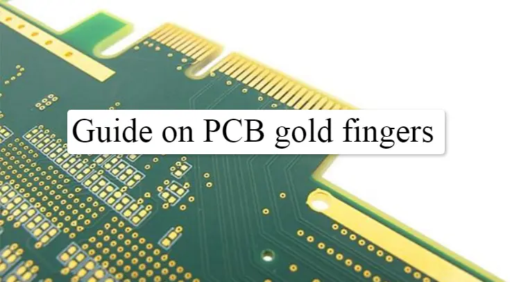
PCB gold fingers
In today’s technology-based world, we all are familiar with the interconnections among different devices. Be it the connection between your laptop and your mobile or the connection between your mobile and Bluetooth headset, PCB gold fingers are liable for all these connections. In terms of connecting the motherboards of two different devices through signals, there are no other options than gold fingers PCBs. As technology is getting upgraded, the necessity for creating inter-connections among different devices is increasing. Naturally, the significance of PCB gold fingers is going upwards.
As you see the structure of a PCB or printed circuit board, you can find tiny columns in the circuit board’s connective edge. Generally, those tiny columns are plated with gold, and that’s why we’re likely to call those columns PCB gold fingers. The usage of PCB gold fingers started for connecting secondary PCBs to the motherboards of computers. However, there is no hard and fast rule that PCB gold fingers will only be used in computer CPUs. In recent days, gold fingers are also being used for connecting other devices like smartphones and smartwatches. In this article, we are going to discuss the types and advantages of PCB gold fingers.
What is PCB gold finger beveling?
Have you found out that the edges of PCB gold fingers are in slope forms? Well, the procedure of beveling allows sharp, square edges to turn into slopes. In the case of PCBs or printed circuit boards, the beveling process completes the surface finish. The beveling process of the gold fingers of a PCB gets initiated after completing the disposition of solder masks. The process of PCB gold finger beveling is unavoidable in terms of making insertions quicker and more effortless. Unless the gold finger beveling is completed, insertions will be more difficult than usual.
As you have already known about the beveling process, you also have to know which angle you are supposed to bevel the edges. Usually, PCB gold fingers are beveled at angles of 30 or 45 degrees to ease up the particular slot’s insertion process. Anyway, engineers and technicians bevel PCB gold fingers according to the requirements of the clients. The beveling angle of gold fingers also depends on the size of a particular circuit board.
Also Read:- Microvias in printed circuit boards
Design specifications for PCB gold fingers
Like other technical devices and circuit boards, PCB gold fingers also consist of specific designs and specifications. The following points will discuss the design specifications for PCB gold fingers. If you’re attempting to create a complete circuit board, these points will better design the gold fingers.
- You must ensure that the inner layers of the PCB are copper-free. The presence of copper in the inner layers of the PCB can generate excess exposure during beveling. Additional exposure during beveling is not expected. Therefore, don’t use copper materials in the inner layers of the PCB.
- Every PCB includes PTH or plated through holes, and those holes need to be posited carefully. The plated through holes of a PCB shouldn’t be posited within a 1 mm area of the gold fingers. There must be at least a 1 mm gap between the gold fingers and the PTHs.
- If you observe the PCB, you will find the main board outline. The board outline and the gold fingers must not be associated, and there must be a gap of 0.5 mm between the gold fingers and the board outline.
- These spacing guidelines are standard, and violation of these guidelines might lead to a malfunction. The design of a gold-plated circuit board must follow these guidelines to avoid malfunctions.
- Every PCB includes solder masks and screen printings all over. But technicians and engineers should keep in mind that no solder mask or screen printing should be nearby the gold fingers. The usage of a PCB that has screen prints or solder masks near the gold fingers is not advisable anyway.
- While setting the design of a PCB, a technician must remember that the gold fingers shouldn’t be facing the center of the PCB. That’s another major thing that has to be followed while creating the design of a PCB.

PCBs with non-inform gold fingers
These PCBs usually include gold fingers that are shorter than the standard size. You will find this kind of gold fingers, mainly in memory card readers.
PCBs with segmented gold fingers

In this case, the sizes of a particular PCB’s gold fingers might differ from each other. Here, all the fingers are not of a similar size. The usage of this kind of PCB is mainly observed in water-resistant electronics.
Quality measures of PCB gold fingers
Every electronic circuit is tested before that is input inside a particular device. Such a circuit board has to go through different performance checks and quality measures. In the following portion, we are going to mention some quality measures of PCB gold fingers.
- The gold plating of a PCB’s gold fingers has to include 5-10% cobalt mandatorily. That certain amount of cobalt in the gold plating allows the gold fingers to gain the expected rigidity.
- There is a strict guideline when it comes to the thickness of the gold fingers. According to the guideline, the thicknesses of the gold fingers of a PCB are likely to be between 2-50 microinches.
- Apart from the above quality measures, visual tests are also performed to judge the quality of the gold fingers of a PCB. The gold fingers of a PCB should be smooth, clean, and those should not contain additional nickel-plating. The visual inspection is generally performed with magnifying glasses.
These are procedures to measure the quality of circuit board fingers, and these techniques detect whether the PCB is useful for inserting into a device.
How are gold fingers changing the world?
As mentioned above, the interactions between the circuit boards and motherboards of different devices are essential for better connectivity. Along with the rapid development of technology, smartphones, PCs, and other devices tend to be faster and more advanced. As technology and connectivity are getting smarter, the importance and significance of PCB gold fingers are increasing. Gold-plated circuit boards are what made the technology as smart as it is currently. With the advancement of time, technology keeps getting more improved and faster. That’s happening due to the improved versions of gold-plated circuit boards. The gold fingers of a circuit board allow insertion and ejection easier and faster. From smartphones to other smart devices, everything is dependent on the functions of the gold fingers. The advancement of gold fingers of PCBs and the enhancement in their performances are what can take the improvement of the smart technology to the next level. The advanced and improved versions of gold fingers enhance the performances of printed circuit boards of different devices. Therefore, it can be said that the gold fingers are liable for the incredible up-gradation of smart technology, and it is changing the global digital trend effectively.
If you are looking for more information about PCB gold fingers or have some questions in your mind, you can reach us anytime. Our experts will offer the best solution according to your specific needs.