


 Get A Quote
  (224)366-0290
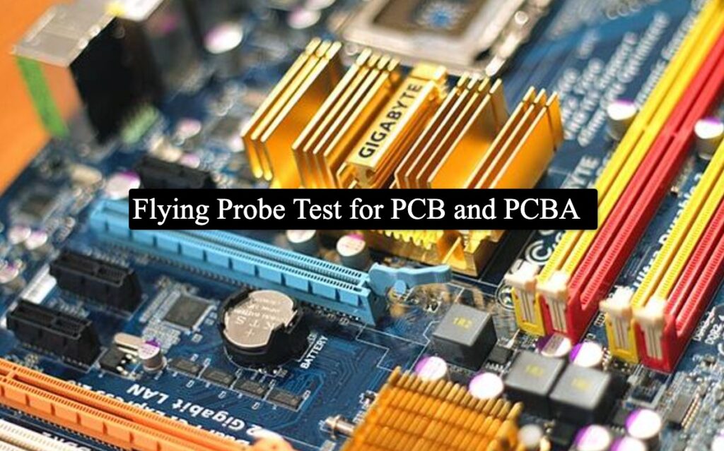
Before leaving the production facility, bare printed circuit boards (PCB) and PCB assemblies (PCBA) are followed by different tests. These tests identify electrical and circuitry problems such as shorts, openings, capacitance, and resistance. Passing the testing ensures that the final products are very reliable and operate well. In PCBA, the two most prevalent testing procedures are Flying Probe Test and In-Circuit Test.
In this article, we will walk you through the essential aspects of the Flying Probe Test. By the end of this post, you will have a thorough understanding of how FPT works and will be able to choose the right Flying Probe tester.
So let’s get started.
What is a flying probe test?
Flying Probe tests are also known as “fixtureless in-circuit testing.” They still utilize probes to evaluate PCB features, but instead of a fixture, the probes are guided to the test locations by software. As a result, the probe “flies” to the place where it is required. Because of its flexibility, this solution is excellent for low-volume and PCBs that are still in the development phase.
Advanced features about testing through the probes
Below we have mentioned some of the rising advanced qualities that make PCB flying probe tests attractive.
These are some examples:
PDM Unit (Phase Difference Measurement Unit): The PDM unit transmits signals to measure the phase difference between various board segments. This feature minimizes the need for unnecessary isolation tests.
HVS Test (High Voltage Stress): If the PDM fails to detect any high resistance isolation faults, the HVS test will run and apply high voltage to the different test locations. This will uncover the problems. According to standard measurements, the maximum application voltage is 250V. HVS, on the other hand, offers significantly greater voltage. It provides variations ranging from 500V to 1000V while also ensuring that the proper amount of power is used to minimize damage to the boards during high resistance testing.
Micro Shorts Detection: It is not unusual for parts with micro shorts to burn out when a high voltage is applied suddenly.
How does flying probe testing works?
The flying probe tester is incredibly simple to use. It’s nearly like using a multimeter to test, check component values, and measure resistance. The probes in the flying probe tester inspect every section on the board to verify the board’s and the components’ intended functionality.
The first step is to develop a test program containing all the necessary information about the PCB, components, and test locations. Then, the plan leads the machine to the probe-testing areas.
After developing the program, it is placed into the flying probe tester for the testing process. The PCB is transferred to the conveyor belt. The test begins when the PCB enters the tester. The tester performs tests on the PCB in accordance with the program that has been placed into it. It uses several signals on the board to test the operation of the components and discover any faults. It gathers all of the information about the PCB and compares it to the benchmark data. This allows it to determine whether the PCB, any circuit, or component is giving the required outcomes or not.
Flying probe testers are used on PCBs and PCB assemblies. First, it detects short circuits and open circuits in bare PCBs by measuring the resistance between the pathways. If there is any defect in the PCB, it gets identified at this step. Next, the flying probe tester checks the functionality of components on assembled PCBs using various electrical signals. The tester also examines the component values; if there is any incorrect placement or a defective component, the tester discovers it. The polarity of the components can also be checked using the flying probe testing machine.
Strength and Weakness of flying probe testing
Strength of PCB flying probe testing
- No fixture is necessary.
- Small-to-medium volume tests for various types of defects at a cheap cost and short time.
- A test program that is both flexible and quick
- There is no need for additional test pads.
Weakness of PCB flying probe testing
- Cannot Test Components at the Same Time.
- Costly and slow for High-volume Production.
- FTP cannot power up a circuit, meaning that a user will not be able to get a true image of the product.
Flying probe test point requirements
While the flying probe test PCB may adapt to a wide range of PCBA prototype layouts and designs, focusing on the following PCBA components can improve test accuracy and reduce the danger of board damage:
Fiducials
The machine requires these reference points for it to know where to put the probes. These are frequently found on the panel waste, but if the trash has been removed, you should consider placing them on the PCB itself.
Board Rail
There should be a border edge on opposing sides that is at least 6mm broad and independent of components for better placement in the machine. This border edge might either represent panel waste or design space.
Components Legs
When probing near component legs, having a dedicated area is essential. To ensure a good solder connection, leave room around the “toe” of component legs and never probe directly on the component legs.
Vias
Vias must not be tented while probing the edge of PCB vias. Therefore, the “non-tented” criterion should be included in your PCB design.
PCB Size
Try to keep the test access points as close together as possible if you work with a large PCB. One of the cons of the flying probe test is that it is pretty slow, with the majority of the time spent moving the probes between measurement areas.
Choosing the Right Flying Probe tester
Consider these critical specifications while selecting the suitable Flying Probe Testers:
- The number of arms
- Number of test steps
- Capacitance
- Resistance
- Inductance
- Probing precision
- Positioning repeatability
- Max board size
- PCB thickness
- System Type
- Open
- Shorts
- Camera
- DC voltage measurement
Lastly, we hope you find this blog helpful, as it has highlighted almost all essential aspects of the PCB flying probe test.