What is LED Driver PCB?
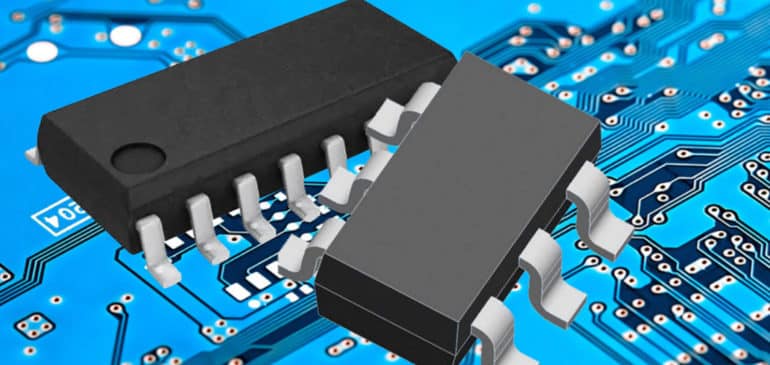
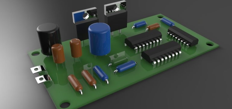
A specific kind of circuit known as LED driver PCB is made for managing and regulating the power distributed to LEDs. Offering the ability to control the flow of electricity to guarantee the highest possible luminosity, lifespan, and effectiveness of the LEDs makes these circuit boards an essential part of LED lighting…
What is Big Switch PCB ?
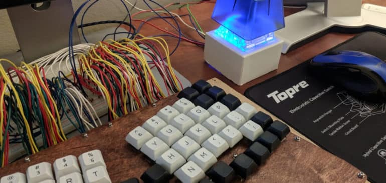
Big Switch PCB A big switch PCB is essential for equipment or devices that require high voltage and power to function appropriately. This type of PCB is created and manufactured to handle high power flow. It is a critical element in regulating and controlling this flow to ensure the safety of the…
What is an Arcade PCB board?
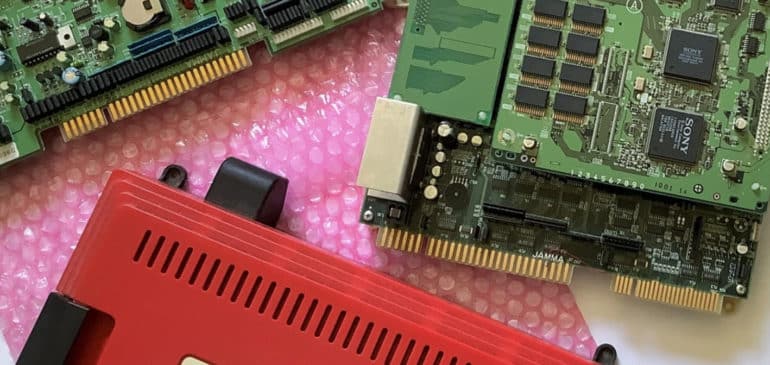
Arcade PCB Arcade PCB Boards are customized printed circuit boards used in arcade devices to hold the game program and manage the electronic components of the games. The central unit handles all player inputs, produces audiovisual results, and controls the entire gaming interface. Customized hardware arrangements are included in an arcade PCB,…
What Cost to Make Custom PCB Printing ?
What is Custom PCB Printing? Designing and producing printed circuit boards, particularly for a particular set of specifications, use cases, or one-of-a-kind electronic gadgets, is known as custom PCB printing. Making a PCB layout specially adapted to an electrical circuit’s dimensions, functioning, and connectivity requirements is known as customization. Custom PCB printing enables…
What is Board to Board Connector ?
Board-to-Board Connector As the name suggests, a board to board connector is a connector used to connect multiple printed circuit boards. In cases where two or more PCBs need to be linked, these components are essential. Board to board connectors enable the flow of electrical signals and currents between the…
How to Design Audio PCB Circuit Board?
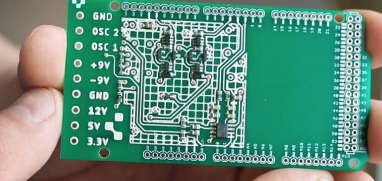
What is Audio PCB ? A circuit board made explicitly for audio electronic equipment is known as an audio PCB. Amplification devices, preamps, equalizing devices, and additional audio processing parts may all be assembled and connected using these circuit boards as the basis. The audio PCB circuit board makes the effective transmission of…
Circuit Printing Easy Way: Machine, Process and Cost
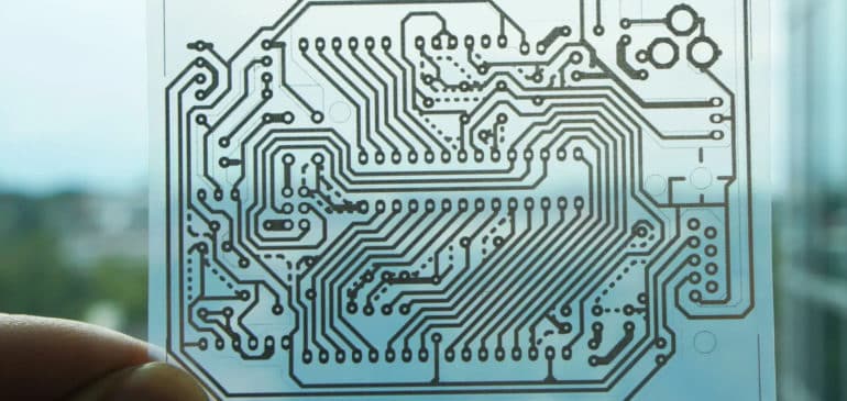
What is Circuit Printing? Circuit printing is using printing processes to create electrical circuits on different surfaces. It is sometimes referred to as printed circuit technology. Electronic circuits could be formed without standard solder or etching because this creative method involves depositing conductive substances or inks upon the surface. In creating…
What is the Difference between LTCC and HTCC ceramic?
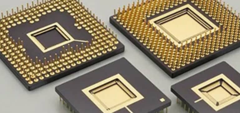
LTCC and HTCC The ceramics packaging methods known as LTCC and HTCC are widely used in the electronics market. The Low-Temperature Co-Fired Ceramic and High-Temperature Co-Fired Ceramic methodologies offer specific advantages, dictating which way should be used for which application. LTCC is vital for incorporating passive elements such as capacitors and entails…
Functions and Characteristics of Amplifier PCB
What is Amplifier PCB? A customized printed circuit board made to hold all of the elements and connections needed for creating radio frequency, and audio amps is known as an amplifier PCB. It acts as the framework for adding numerous parts required to complete the amplifier circuit. The amplifier PCBs are a…
Exploring the Facts of PCB Printing Services
What is PCB Printing Service? PCB printing services are expert production and creation services that create printed circuit boards with unique designs per predetermined specifications. These solutions include printing conductive lines on insulation surfaces, among other methods, to produce printed circuit boards (PCBs). Various alternatives, including single-layer, double-layer, and multilayer circuit…

