


 Get A Quote
  (224)366-0290
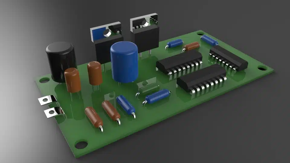
What is Audio PCB ?
A circuit board made explicitly for audio electronic equipment is known as an audio PCB. Amplification devices, preamps, equalizing devices, and additional audio processing parts may all be assembled and connected using these circuit boards as the basis. The audio PCB circuit board makes the effective transmission of signals and electrical links essential for obtaining high-quality sound output possible by helping with the circuitry’s structured layout. These PCBs are vital in producing audio components to provide dependable and optimal device performance.
Elements of an Audio PCB
- Sound-related Parts: Audio elements like inducting parts, resistors, etc, are critical for audio PCB. These parts are set up for filtering and shaping the audio signals, thereby improving output. Electrical energy is stored and released by capacitors, inductors filter out undesirable frequencies, and resistors regulate the movement of the electrical currents.
- Operating Amps: The minimum distortion of sound signals in audio PCB is achieved using operating amplifiers, also known as Op-Amps. These are a crucial part of the development of audio amps, along with other audio processing systems, while also boosting the power of the input signal.
- Diodes and Transistors: Diodes offer correction and regulate the course of the current in the circuit, guaranteeing correct signal circulation, whereas transistors enhance and regulate the movement of sound signals. These essential functions form a vital part of the audio PCB.
- Connections and Endpoints: The audio PCB circuit board is capable of interacting with external gadgets, including mics, speakers, and other audio gear, due to its output and input connections, which make it easier to link audio source points to the output points.
- Power Supply Elements: Unnecessary disturbances and noise are avoided by using components like rectifier devices, capacitors, and voltage regulation devices. These elements are pivotal in providing a steady and pristine electrical supply to an audio PCB circuit board.
- Signal Tracks and Pathways: Audio impulses go through electrical lines on the printed circuit boards, connecting the various elements. Appropriate sequencing and audio PCB design are essential to reduce disturbance and preserve signal integrity.
- Safety Circuitry: Protective elements such as fuses and surge safeguards can be incorporated to prevent harm from occurring to the audio PCB circuit board through electrical surges or other unanticipated occurrences.
- Integrated Circuits: Unique integrated circuits (ICs) explicitly made for audio-related purposes are called audio ICs. Analog-to-digital converters (ADCs), digital-to-analog converters (DACs), and additional processing devices commonly incorporate audio ICs in an audio PCB.
- Volume Regulators: Audio output loudness is controlled using potentiometers, commonly called volume controls. Customers can alter the sound output’s intensity with these movable resistors included in the audio PCB design.
- Grounding Mechanism: Reducing disruptions and noise requires a meticulously planned grounding mechanism in audio PCB. As a result, there is a reduced chance of ground loops occurring and establishing an uninterrupted point of reference for the sound impulses.
- Equalization and Filtering: The range of frequencies of the sound stream can be modified by adding more parts on the audio PCB circuit board, such as equalization devices and filters, which change the treble, bass, and other characteristics.
How to Create Audio PCB Design
- Part Orientation: Component placement should be done deliberately to shorten signal paths and lower the chance of contamination. Put similar parts in a single arrangement and consider how the sound signal travels throughout the audio PCB circuit board.
- Signal Routes: To reduce the deterioration of signals on the audio PCB, keeping audio signal pathways as brief and straight as feasible is a vital and effective strategy. High-current and delicate audio signals should be routed on separate tracks from digital or electrical lines.
- Protection: To minimize radio-frequency interference (RFI) and EMI (electromagnetic interference), it is essential to implement shielding measures, including grounding planes or shields surrounding parts that are delicate on the audio PCB.
- Evaluation Points: For ease of access throughout the prototype and evaluation stages, it is important to incorporate testing locations within the structure of the audio PCB circuit board design. The assessment of important metrics and debugging are made easier through these spots.
- Grounding: It is essential to adopt a strong grounding approach to reduce distortion and avoid ground looping on the audio PCB. To lessen the possibility of ground-related problems, employ a star-grounding strategy in which all ground points merge at the same node.
- Power Supply Configuration: Position the power source’s elements adjacent to the sound circuit to shorten the total length of the electrical traces on the audio PCB. Use the appropriate decoupling capacitors to eliminate noise at high frequencies and provide a steady power source.
- Division of Digital and Analog Segments: To avert digital interference from influencing the delicate analog sound signals, the audio PCB circuit board should have distinct areas dedicated to both digital and analog functions. Keep sensitive analog parts such as digital signal processors and microcontrollers far away from each other.
- Thermal Transmission: Think about the heat that various parts of the audio PCB circuit board produce. Heat-generating elements should be positioned carefully to promote effective heat dispersion and prevent thermal problems.
- Element Positioning: Always align the elements in the same direction to keep the audio PCB arrangement orderly. Ensure all the element’s marks are evident for simple debugging and that the polarized elements are positioned appropriately.
- Track Size and Match Resistance: According to the existing needs of the audio PCB, determine the optimal tracing widths for audio signal transmission. Transmission lines should consider the resistance match to avoid irregularities and bounces.
- Routing Methods: Use appropriate routing approaches to guarantee signal integrity and lower the possibility of undesired capacitance, like eliminating sharp edges in trails and keeping trace widths stable.
Designing an audio PCB circuit board can be a challenging task; however, when done after careful layout planning, a highly effective circuit board can be created. Since they impact the sound-based electronic industry so critically, it is essential to follow best design practices.