


 Get A Quote
  (224)366-0290
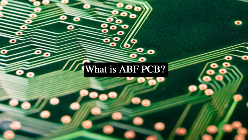
The Ajinomoto Group is not famous for only offering components of computers. They are the heart of personal computers across the world. The term “ABF” is a short-term for Ajinomoto Build-up Film. Moreover, this type of film consists series of film dielectrics. The dielectric thin film provides the electric insulation of the circuit substrate for ensuring the high performance of the CPUs.
The ABF PCB is an essential component in chip manufacturing. Since the development of the ABF PCB, it has been widely used for chip manufacturing. The substrates comprise the ABF film generally found in base stations, routers, and personal computers.
The ABF has had a long history dating back to the 1970s. The ABF was initially integrated into personal computers in the 90s. It has then continued to evolve.
Challenges In The ABF PCB Market
The ABF PCB market will grow with better revenue in the coming years due to the robust demand for servers and 5G networks. Moreover, the car industry’s strong demand for high-performance computing and graphic processing units has contributed a lot to its increasing revenue.
Goldman Sachs stated that the aggregate demand for the ABF substrates should be up to a CAGR of 28%. Moreover, there is also a short supply of ABF Substrates. The rising demand and supply chain issues will contribute to the storage of the ABF PCB. Additionally, the rising numbers of larger pack sizes and layers for these high-tech products highly contribute to the shortage.
In the long term, these bigger and larger packaging sizes will lead to fewer packages for every ABF substrate. Moreover, the ABF PCB manufacturing process consists of build-up layers. Hence, any issue in the layer can neutralize the outcome of the whole ABF Substrate.
Yield controlling is an essential project that accounts for the steps involved in the ABF process. Moreover, the ABF PCB suppliers have relied on the ability to repair the RDL defects to enhance the yield. However, the high-performance chips in smaller sizes of the RDL will make the repairing process challenging.
Intel stated that an additional challenge of the manufacturing of ABF PCB is that there are decentralized films. For example, capacitors are the major elements of the ABF Substrate. They are widely used for decoupling.
What Does ABF PCB Do?
The ABF substrate is amongst the essential components of the manufacturing process processing units. Today, semiconductor-based processing units are widely integrated to get to the nanometer processes. Due to this, the interconnection information has become complicated.
Moreover, the interconnecting electronic systems level and board are popular on the millimeter scale. Hence, to achieve these interconnections, most semiconductor manufacturers must integrate the ABF. Moreover, the ABF serves the purpose of bed within the packaging of a device. Moreover, it also comprises several layering of the microcircuits that interface between the nanoscale PCB and CPU.
The Ajinomoto Group also designs the thermosetting film, which provides insulation to the processing unit. Moreover, this film has crucial properties such as high durability and low thermal expansion.
What Are ABF Substrates?
The ABF Substrates are primarily used for making the ABF IC carriers that are made by Intel and are currently monopolized by the famous Ajinomoto and are used for producing high-end substrates such as FC.
How Has ABF PCBs Affected The Semiconductors Manufacturing?
Semiconductors are the ICT infrastructure’s basis. Moreover, the downsizing of the semiconductor and multifunctional performance of high-level enables smarter mobile phones and related devices. Moreover, it will enable functions for the communication, safety, and control of several devices in automobiles and houses.
The Ajinomoto Group also keeps on improving the technology for the ABF Substrates. The specialization will also assist in driving further downsizing and spreading the semiconductors. ABF is essential in many factors, so its evolution will transcend society.
ABF substrate is an essential component for chip making. Moreover, it is the most recent issue for electronic firms that are going through shortages of semiconductors. The ABF substrate is a vital packaging part that shields the chips needed to power a car or computer.
The most advanced semiconductors in the globe cannot work without substrates. Hence, most giant companies, such as Intel, are spending billions of dollars in reducing chip shortages, and the shortage of ABF substrate can affect the manufacturing process. Due to the limited capacity, there will still be supply constraints.
Most semiconductor companies, such as AMD and Nvidia, rely on the ABF substrates to make the world’s most powerful chips. However, the substrate manufacturers are reluctant to invest in the capacity because of the money-losing slumps they have experienced.
Moreover, introducing the 5G has amplified the demand for stronger server chips that can handle cloud computing, AI, and other smart-driving technologies. The ABF substrate was first integrated as the ideal packaging technology for the CPUs in personal computers and servers. It is because it enhances faster computation by the high-end chips.
The ABF substrates have different uses and are available in different materials. Such as the Flexible substrate has the main materials and application areas of PE and PI that are applied to automotive electronics and customer electronics that can also be used in the military fields, such as cruise missiles, launch vehicles, and space satellites.
On the other hand, the hard substrate comes with BT resin used for memory and communication chips and LED chips. The ABF substrate is applied to many high-end chips such as chipsets, CPUs, and GPUs. The MIS is applied to the power IC, analog and digital currency, and many more.
The ceramic substrate materials and applications in alumina silicon carbide are used in laser, semiconductor lighting, optical communication, automotive, aerospace, deep sea drilling, and many other leading fields.
The Use Of Inorganics and Organics In Microfilm
The advent of the resin composition, which determines the functioning of the insulation material, is the primary objective of the R&D which resulted in the ABF. The experience of the Ajinomoto Group in chemistry was integrated for creating a formulation that consists of microparticle filler, hardener, inorganics, and organic epoxy resins.
Moreover, the primary challenge was formulating the methodology for combining the organic and inorganic substances and providing great insulating properties. Hence, the R&D team has made the thermosetting film to overcome these challenges. Moreover, this thermosetting film features low thermal expansion, ease of processing, and high durability.
The film was first integrated by the semiconductor manufacturer in 1999. After its integration, this film has become a highly preferred product for every high-performance CPU. Moreover, this film has evolved to meet the rapid development demands in circuit integration.
Furthermore, circuit integration has led to the development of CPUs with nanometre-scale electronic circuits. Hence, it needs the integration of the R&D in the insulation of the resins with the processing technologies to meet customers’ needs.
Conclusion
The ABF PCB market will continue to grow over the years. The G5, AI, and HPC will primarily drive the market. Moreover, the ABF Substrates manufacturer will benefit from the demand for the increased capacity. The IC substrate suppliers plan to allocate a portion of the SLP to help manufacture the ABF substrate. By reading this article, you have learned what ABF is and how it benefits the industry.