


 Get A Quote
  (224)366-0290
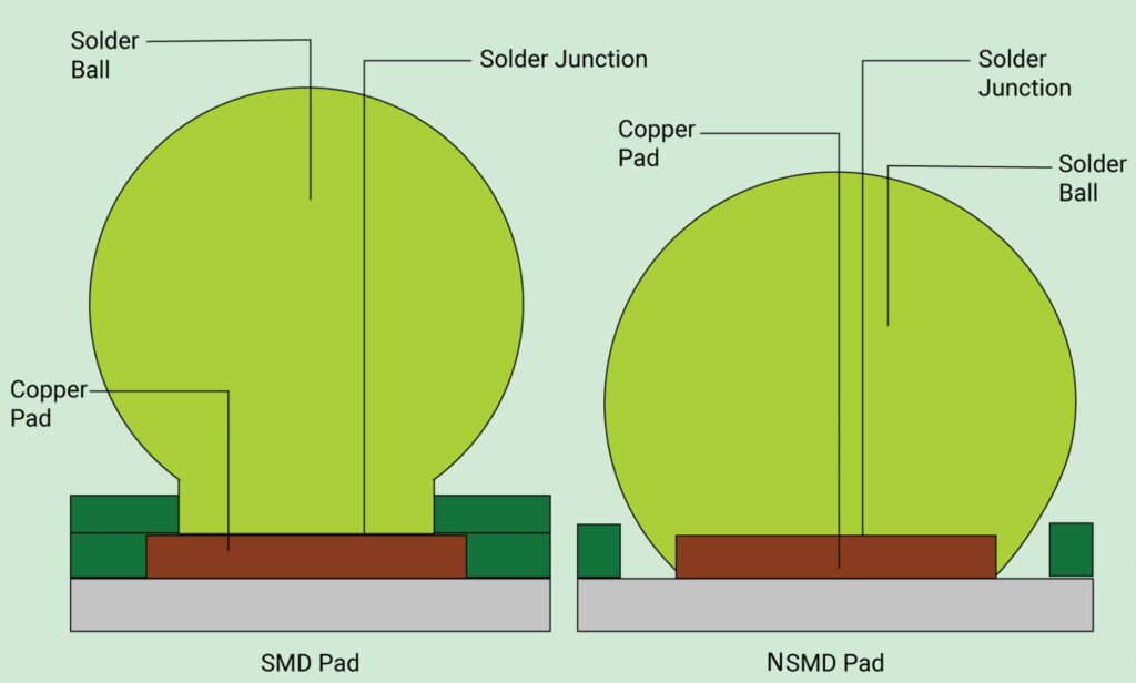
Printed Circuit Boards are vital components in modern electronics. They serve as the backbone of electronic devices and are responsible for routing signals and power between components. PCB design and development involve creating the board’s layout, selecting the appropriate components, and designing the interconnections between them.
In this blog, we will explore the different types of pads used in PCB Design, their importance in the overall functionality of the board, and best practices for designing and placing pads in your PCB. No matter if you are new to PCB Design or a seasoned professional, understanding the role of pads in PCB Design and development is essential to creating reliable and high-performance electronic devices.
What are pads in PCB design?
The uncovered metal area on an electrical circuit board where the factor lead has been soldered is known as the PCB pad. Aligning aggregate pads creates the component footmark PCB design model. There are mainly two types of PCB pads:
Surface mount pads
Surface mount pads are PCB pads that are used to mount surface mount components. The following are the main features of these pads:
- Solder mask layer
- Solder paste
- Pad number
- These PCB pads represent copper areas in several shapes, like rectangular, round, square, and more.
BGA pads are printed circuit boards’ most commonly used surface mount pads. Below are the primary features of these pads:
SMD and NSMD pads
Proper PCB Design is crucial for the manufacturability of BGA components. There are two kinds of BGA pads, which are solder mask-defined and non-solder mask-defined pads.
SMD BGA pads:
The solder mask aperture applied to the BGA pads defines the SMD pads. These BGA pads have solder mask apertures that are smaller than the pad diameters they are covering. This is performed to shrink the PCB pad sizes of the copper.
NSMD pads:
NSMD pads are distinguished from SMD pads because the solder mask is defined not to contact a copper pad. The mask is created in such a way that a gap is created between the solder mask and the edge of the pad.
Through-hole pads:
The pads used to cover through-hole components are called through-hole pads. There are two types of through-hole pads. Below are the types of these pads:
Plated through-hole pads:
Plated through-hole pads, or PTH pads, are through-hole pads. The entire wall will be plated with copper and, occasionally, solder or defensive plating. The electrolysis procedure is used to create the hole plating. The metal plating allows electrical connections with different levels of the board.
Non-plated through-hole
Non-plated through-hole pads, also known as NPTH pads, are pads without plating in the hole. This type of pad is employed for single-sided circuit boards; alternatively, these holes are employed to put the PCB into an enclosure, and chicanes can be put through these holes. Unplated holes will eventually hold a region close to the clean-cut hole of moderate copper (standardized to circuit board edge headway). This is done to prevent a gap between parts and the copper layers that are situated.
Can you put a via on a pad?
Wherever space is limited in HDI patterns, it is necessary to place vias on pads. Conventional vias come with signals and traces routed away from the pad and via. Via-in-pad reduces the space used by trace rooting to reduce the form component of a PCB pad. These pads are used for BGA elements with pitches of less than 0.5 mm.
What is a bond pad?
A bonding pad serves the primary purpose of connecting the circuit on a die with the pin on packaged chips. The single side of a gold cable connects to the bonding pad. At the same time, the opposite sides will connect to the box. The bond pad comprises all the metallic layers piled on top of one another and connected by vias. This allows for connection from the chip core to the PCB pad.
The die also needs a passivation layer or insulator to protect the core from environmental or weather contamination. The non-conductor layer cannot cover the bonding pads, which must be visible for connection to the chip box. The layer of glass is employed by the manufacturer where the opening is required to be bonded.
What is via plugging in the PCB?
Via plugging is a method for filling vias with resin or closing them with solder masks. This method differs from via tenting because resin or solder masks do not fill the via hole. It only provides cover. This technique is employed to protect the vias from the undesirable flow of the solder throughout the soldering process. The solder can flow into the via from the pads when the via is not plugged. It leads to the creation of unwanted solder joints.
Via plugging can be implemented with the help of non-conductive or conductive material. Conductive material help in conducting current from one to another side of the board. While the printed circuit board is in operation, the conductive material will heat faster than the surrounding laminates, expand, and cause a fracture. Via holes that are filled with non-conductive material can work as usual via. But it will not carry a high current as a conductive material does.
Errors in Manual pads design
Nowadays, the mechanism is used to remove the pad’s manual pattern. Pad manual PCB Design includes designing the required pad shape with the help of PCB design software tools. This can be represented with the help of formulas and datasheets for general pad size and shape.
Hand-operated procedures are prone to errors because fabricator specifications do designers adhere to formulas as they do in automated systems. It leads to designing pcb pad sizes and shapes, which leads to undesirable results like:
-
Through-hole breakout
Through-hole pads need a robust, rounded ring for soldering. The metallic component between the pad’s external border and the hole sounds is the spherical ring. The spherical or angular ring must be large enough to compensate for the drill from the hole center. If the PCB pad size is compact or small, it could cause a breakout, resulting in broken or incomplete circuits or soldering.
-
Insufficient solder joint
SMT components with tiny pads may not receive a suitable solder stopping during soldering. The deficiency of delicate fillets can lead to a weak solder joint that can break.
-
Floating parts
SMT factors obtained on large pads compelled the solder reflow procedure. This might lead to a gap between electrical circuits.
-
Tombstoning parts
SMT factors with two more compact leads defined as resistors and condensers can have consequences because pads are not the same size. This error where one PCB pad will heat faster than the other is known as tombstoning, as the factor will draw up from the other pads, facing like a tombstone.
Conclusion
Pads are integral to the PCB Design and development process. These small conductive areas are critical in connecting components to the rest of the circuit and routing signals and power between them. By understanding the different types of pads and their impact on the board’s overall performance, designers can create reliable and efficient electronic devices.