Single Sided PCB Manufacturer
In a layperson’s language, we can define a single sided PCB as a one-layer PCB, where all electronic components are on one side of the board and all circuits on another layer. It is noteworthy that single-sided PCBs comprise a solo layer of conductive material and are ideal for low-density designs. A single-sided PCB design is restrictive and, therefore, primarily utilized in rudimentary PCBs. However, since their inception in the 1950s, single sided PCBs still dominate the global market in terms of sheer piece volume. The continuing popularity of a single sided printed circuit board can be attributed to its workable design, cost-effectiveness, and quick manufacturing. After a crisp overview of a single-sided PCB, it is time to understand its production process.
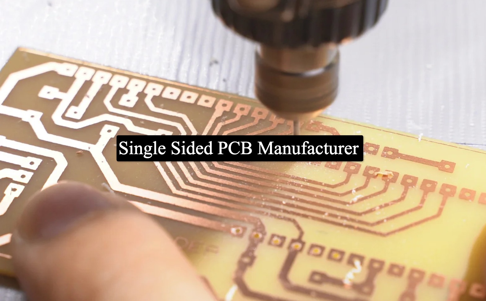
HOW ARE SINGLE SIDED PCBS MADE?
Owing to its simple design, a single sided PCB is easy to make. A single-sided PCB’s substrate consists of fiberglass to increase the board’s strength. On the substrate, different paths for current flow coupled with various components are assembled with the help of copper, which is affordable and the best conductor of electricity. After that, a solder mask layer is coated over the copper conductive path to protect it from corrosion via oxidation and environmental moisture. Ultimately, a third silkscreen layer is employed above the two copper and solder masks to illustrate different components, symbols, etc., and ensure that the users position the components at the right place with the apt connection. All the single sided PCB manufacturers utilize the aforementioned technique to produce their circuits.
BENEFITS OF SINGLE SIDED PCBS
Let us look at the top four factors that offer single sided printing circuit boards an edge over the rest.
- Low Cost – The primary benefit of a single sided PCB printing circuit board is its affordability. Due to rudimentary design and structure, single sided PCBs need less material, time, and practical experience, thereby making them pocket-friendly. This variant of PCB is ideal for high-volume orders.
- Short Lead Time – It takes significantly less time to produce single sided PCBs. Thus, they are optimal for companies that want bulk PCB orders at urgent notice.
- Accessible Design – The design and construction of single sided PCBs are so simple that any novice designer can construct them without much hassle. It is also possible to DIY a single sided PCB, but with discretion.
- Minimal Glitches – the simplistic structure of a single sided PCB printing circuit board implies that the chances of manufacturing and issues decrease considerably.
SINGLE SIDED PCB TECHNOLOGY
| ITEM | CONTENT |
| Material Type | XPC FR-1 FR-4 CEM-1 |
| Surface Finish | HASL Immersion Tin, ENIG gold, Chemical Silver OSP |
| Layer No. | Single Side, Multilayer PCB |
| Maximum PCB Size | 1500mm x 600mm |
| Minimum PCB Size | 5mm x 5mm |
| Minimum Space or Width |
|
| Board Thickness |
|
| Warp and Twist | Greater than 0.5 percent when the board thickness is 1.6 mm, PCB size is 300mm x 300mm |
| Copper Thickness | 35um-240um |
| Outline Tolerance | ±0.15mm |
| V-CUT Precision | ±0.1mm |
| Capacity | 80000㎡/Month |
| PTH Dia Tolerance | ±0.076mm |
| Outline Tolerance | CNC:±0.1mm punch:±0.15mm |
Now that we covered the technicalities of a single sided PCBs, let us look into its maintenance.
HOW TO MAINTAIN SINGLE SIDE PCB?
The maintenance of a single sided PCB depends upon understanding the failure situation.
- Board Observation – It involves preliminary research to understand the input and output interfaces of the board, the functions it implements, and the distribution of various control parts of the board.
- Circuit Test – After completing the board observation, you have to initiate a circuit test to grasp its faulty point. However, the initial test may not yield satisfactory results, and calling a professional might become necessary.
- Component Inspection – The element of maintaining a single sided PCBs is to remove the components from the circuit with soldering equipment and inspect them with professional tools.
- Fault Maintenance – The maintenance steps are curated to deal with faults, such as line repair, component replacement, transformation, etc.
- Computer Test – Lastly, the board maintenance is completed when it is tested on a computer, and we can confirm there are no more faults.
Now let us quickly skim through the salient features and applications of a single sided printed circuit board.
SINGLE SIDE PCB APPLICATION AND CHARACTERISTICS
- Excellent Reliability – A single sided PCB can work reliably for 20 years with proper maintenance.
- Workability – The single sided printed board can be designed in a short time with efficiency.
- Testability – We have various instruments such as test equipment and methods to measure the eligibility of a single sided PCB
- Standardized Assembly – A single sided PCB manufacturer finds it easy to assemble several components of a single sided PCB and automate the process for large-scale mass production.
- Consistent Production – It is feasible to deliver standardized, scaled, and automated single sided PCBs for consistent product quality in the manufacturing process of single sided PCBs.
- Easy Maintenance – The final characteristic of a single sided printed circuit board is that it is easy to maintain, as component replacement is quick.
We can find the application of single sided PCBs in different devices, such as –
Power supplies
- Timing circuits
- Relays (automotive and industrial)
- LED lighting
- Radio and stereo equipment
- Sensor products
- Surveillance
- Packaging equipment
- Calculators
- Printers
- Vending machines
- Coffee makers
- Surveillance
- Solid state drives
- Camera systems
After observing the nitty-gritty of single sided PCBs, it is time to understand its proofing design process.
PCB SINGLE-SIDED PROOFING DESIGN PROCESS
- The preparation part includes completing a schematic design
- Specific operation part wherein you have to import all the package files and netlists into the PCB file with the frame
- Fixing devices such as LEDs, buttons, deck, etc. at their correct installation position
- Carrying out a general layout to determine the location of each functional module
- Completing the placement of each corresponding device for each functional module
- You have to wire the components
- Align the power cord
- Floor treatment where you can find a large ground plane equivalent to completing the wiring of the ground wire
- Adjust the device layout
- Check the drawing specifications of all PCB boards
- Expert the PCB with the format Protel PCB 2.9 ASCII File
- Finally, send out the PCB for design proofing
There we have it, a twelve-step regiment of the single sided PCB proofing design process.
CHOOSE US AS THE BEST SINGLE SIDED PCB MANUFACTURER
Although there is an inundation of single sided PCBs, finding the right manufacturer can be tricky. If you are looking for someone trustworthy, then Absolute PCB is a company worth considering. With 20 years of experience in the circuit industry, Absolute PCB only resorts to the best manufacturing process for single sided PCBs.