


 Get A Quote
  (224)366-0290
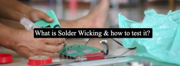
What is Solder Wick?
Solder Wicking is referred to as when the solder gets flown away on a PCB from the pad. This further leads to dirt getting accumulated on the surface that leads to holes and tracks. The component terminal comprises a melting point that is a lot lower as compared to the pad where it is being soldered. Hence, the component terminal tends to reach the melting point prior to the pad and the solder flowing away and tending to accumulate in unnecessary areas.
Evaluation methods of wicking:
The process is measured once the plating of the test panel is done. The processed holes are further examined to get the measurement of a high level of wicking. The Solder wicking is further confirmed clearly whenever a cross-section is performed at 90g. This distance is the baseline of the wall to the last point of the ingress.
When you fail to measure the wicking, then it might lead to a faulty result. The measurement needs to start and stop where the solder wicking starts and ends, and only then will the results be completely accurate.
The standards and norms for the specifications of the production need to be spontaneous. This will help you acquire a modern production meeting the present-day demands. It needs the right dedication, hard work, and constant attention throughout the production process.
It is recommended to extract knowledge from the production files while converting it further to data that can be utilized later to improvise the standards. This helps to meet the demands as stated by the PCB and of the industry at large.
PCB Wicking Cause Reason:
A lot of you might be already wondering about the reasons for a poor solder joint on the PCB. If you are confused about it, you must know that the solder paste tends to get redirected on the PCB from the pad during Reflow. This is referred to as solder drainage, solder wick, or solder escape.
This takes place due to the following reasons:
- Copper areas
- Holes
- Larger tracks
- Animation of a via hole
Being situated too close to the SM pad, hence it does not have any solder mark dam to protect the solder paste from evading in the hole.
PCB wicking solution:
The PCB assembly challenge involves attaching a panel to one significant side of a pad with the help of solder paste. This is done by using an SMT reflow soldering oven.
PCB wicking 1:
PCB Solder wicking venturing through unmasked vias goes to backside emerges as being unacceptable bumps on top of vias.
Although the bond or attachment was not the issue, however, post the first trial, it was evident that solder wicking was going to take place through the unmasked vias. This can be done to safeguard the solder where it is expected to stay at the reflow time. This was when it was necessary to find a way to prevent it from wicking up.
It was necessary to acquire a temporary however simple solution which withstands reflow soldering temperature. The perfect solution to the problem was Kapton polyimide tape, a popular product used in PCB assemblers. The best thing about the product is that it does not degrade at reflow temperatures.
Kapton tape-Molden solde:
This is used to cover the unmasked vias. If it is not covered, it might block the modern solder from getting leaked. The Kapton tape is applied to cover the unmasked vias to block molten solder from cooling and leaking. This is a temporary solution found, which an affordable and user-friendly solution is.
Temporary masking solution PCB:
This is a temporary method that works with no solder bumps on the backside.
How to prevent solder wicking?
- The pad reaches the temperature a lot later as compared to the lead. Hence, the melted solder gets tightened well by the lead.
- The solder alloy gets pulled to the hotter surface when there is enough wettability
- Leads tend to melt faster as compared to the river solder joint.
- This delays liquefaction of the solder paste tends to pull the leads away from the pads.
- The non-wetting concerns such as thin plating or oxidation can lead to wicking-up.
Here are a few conceivable wetting parameters:
- Wettability of pad
- Temperature difference
- Melting time of solder
- Heat sink at the conductor
The heat sink needs to be heated at first, while high convection heat needs to be applied.
How can Absolute PCB Team help you?
Whenever you are looking at testing solder wicking and exploring the wicking evaluation methods, you must seek professional assistance from the Absolute PCB Team. With the help of expert assistance, you can attain the right guidance. Feel free to get in touch with the experts to test solder wicking and explore wicking solution.