


 Get A Quote
  (224)366-0290
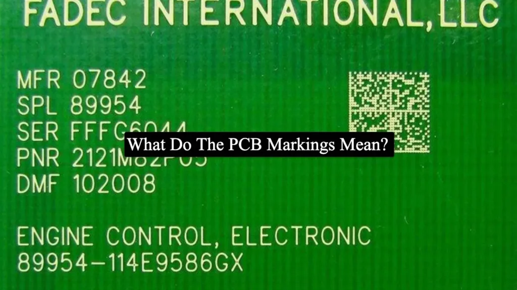
Today PCB or the Printed Circuit Board has become a revolution in the world of electronics. Such is the popularity of the electronic circuit that it has become the prime face of all types of equipment across the globe. But what makes these boards so unique?
Well, PCB boards are proportionately sized, convenient, lightweight, and have good strength when compared to other circuit boards. Moreover, the multilayer boards manufactured today have the opportunity to connect small elements easily.
When we take a look at the PCB board, we can see a lot of markings engraved over it. These PCB markings play a very important role as they help identify special elements easily. Most of the common types of marking used on a PCB include etching codes, numbers, and logos.
However, today the marking on the PCB has evolved. The automated laser markings used today mitigate extra processes and easily integrate with SMT lines. This makes the boards reliable and helps the manufacturer enable real-time tracking.
Also, the use of laser markings doesn’t involve chemicals and is a contactless process which makes the method cost-effective. Due to the various benefits associated with this type of circuit board markings, manufacturers are increasingly gravitating towards these solutions.
What Are The Types of PCB Markings?
Despite being surrounded by different types of electronic devices, the world of technology remains a mystery for us. The same thing goes for a PCB. The board forms the crux of millions of gadgets and has some basic markings, which are important to learn. Let us check out what they are.
Mark Point:
The Mark Point of PCB is also known as the reference point. It is the main point of the positioning where the SMT machine is used. We all know that PCB products form the common measuring points in the assembly of mass productions.
This means every PCB marker allows the machine to be automatically set by the programmer. As the mark point forms the focal area of the whole circuit, it is one of the distinguishable features of the board.
Mark Point Design Specifications:
When we take a closer look at each PCB board, we can find at least a pair of marks on every one of them. These points are essential, and at least every PCB board shall have one pair of them. This is because the mark or the combination of marks serves as the auxiliary position and is important for each board.
Shape and Design Specifications of The Mark Point:
The Mark Point is used as a position of the machine’s placement or as a part of machine identification. Usually, it is seen that the mark point can be drawn in different shapes such as round, square, triangular, and diamond.
Apart from these, there are other specifications in the PCB board which form the basis of markings. They include a capacitor, diode, and polarity marks. All these together form the circuit board codes, which are then used by manufacturers for a better understanding.
What is the role of Marks?
The mark points that we see on the PCB board are also known as Fiducial points. These form the common and localized circuit pattern in all steps and the overall assembly process. While there are many PCB symbols, the mark point is one of the common parameters that is used in SMT production.
Different types of Mark Points and their explanations?
Single board mark:
This particular symbol represents the positioning of all the features on the circuit on a single board.
Puzzle mark:
The Puzzle mark is used to locating circuit features and their positioning.
Local Mark:
Local Mark is used to locating a single component and improve overall placement accuracy.
The role of Mark Points in PCB is rather conceptualized and precise. They are used for the automatic placement of the board in the circuit design. Also, it is seen that the PCB mark point is known as the reference point. It is because this particular point acts as a common measurable point and helps in the accurate positioning of the PCB components.
When we consider PCB assembly, then these fiducial markers play a key role. This is because they are oriented in the correct direction and have been aligned as close to perfect. There are also some tips for placing these fiducial marks:
- The marked point shall be of optimum size and must fall in between 1 mm and 3 mm.
- The marked point must be clear and free of any solder mask.
- All the fiducial points must be located opposite to one another.
- If there is insufficient spacing, then one global fiducial marker is enough.
- The marked point shall be placed at a distance of o.3 inches to the edge of the board.
Shape and design specifications of the Mark Point
As we all know the fiducial marks forms the basis of a PCB board, there are certain specific design and requirements which has to be met. First of all, one shall be very clear about the need for a marking point.
The marking point in the PCB is used either for positioning the placement machine. There are several shapes in which mark points are drawn. They can be triangular, diamond, round, or any other identifiable shape.
The shape is used as the crux to position the board in the machine correctly. When it comes to the average diameter of the mark, it shall not exceed beyond 1.0MM. The mark also consists of two areas, namely open area and mark.
Another thing to keep in mind is that every marked point in the PCB shall be asymmetrical and the same. Both of these help in the assembling of the PCB and thus cannot be changed. When it comes to the recognition of machine and other PCB component codes, then the mark points also play a key role.
Also, to make the overall board look effective, two mark points must appear in pairs. Apart from the mark points, there are other PCB layouts also to keep in mind. Several features come under these:
- Switch Nodes:
The Switch node is an electrostatic radiator present in the PCB circuit. Its function is to allow free current flow and discharge the capaciousness between the node and the ground planes.
- Input Capacitor Bank:
There are two capacitor banks in the PCB. One is the input capacitor bank, and the other is the output capacitor bank. The main function of both these banks is a power-factor correction from devices such as transmission lines and electric motors.
Call to action:
Thus, if you need to avail yourself of the best PCBs, then there is one company to trust, and it is Absolute electronics services. We are known for its top-quality manufacturing PCBs and hence provides the best of goods to you. One of the prime aspects that demarcate the company is its efficient and highly-trained staff.
Thus, what are you waiting for? Contact us right now by either dropping an email or giving us a call. In this way, you can be assured of getting the best service from the professionals.