


 Get A Quote
  (224)366-0290
 Compact, low-power gadgets have long been favored due to customer desire for high-tech capabilities in tiny containers, especially in automotive and smart wearables. There is a high demand for PCB antennas nowadays to allow reliable connections for devices like wireless mice, the upcoming 5G network, and the Internet of Things because wireless devices are quickly becoming the norm for most applications. Additionally, PCB antennas’ high strength and network compatibility make them solidly connected and lasting, enabling most consumer electronic gadgets to incorporate them. Due to the necessity for a wireless connection, a PCB antenna will be crucial in expanding and creating communications.
To learn more about PCB Antenna, continue reading the blog below.
What is a PCB antenna?
To create electromagnetic (EM) waves on a high-frequency PCB, a PCB antenna has been introduced as a transducer. High-frequency electricity is transformed into airborne electromagnetic waves by PCB antennas. A PCB for high-frequency devices has two PCB antennas. They are etched copper structures that are included in the PCB. While the other antenna serves as the receiver of the reflected radio frequency signal, one antenna transmits the signal. The circuitry on the circuit board’s base materials carries the signals to the PCB antenna after the high-frequency circuit creates RF waves and analyses the signals made by reflected RF waves. The entire RF system of the high-frequency PCB is composed of the PCB antennas and the high-frequency circuit.
Since the PCB antenna is intended to be extremely tiny and compact, numerous microstrip patches are integrated to maximize efficiency to obtain the needed gain from the antenna’s smallest possible size. A directional PCB antenna only needs to send its signals in one direction, as opposed to an omnidirectional antenna, which may do so. Semi-directional is defined as having a predetermined propagation angle for the signal.
Types of Antennas
Antennas are used to create high-frequency PCBs, and PCB antennas are integrated into them. PCB antennas exist in a variety of sizes and forms, and since they have so many uses, designing them is essential. Several aspects must be considered while using PCB antenna design approaches. Understanding the different types of antennas is necessary before one can realize how PCB antenna design, exhibit, and function.
-
The Loop Antenna
The loop antenna is the most basic kind of PCB antenna. The receiver or transmitter terminals are linked to the PCB board’s closed loop. The antenna may resemble a loop, either round or rectangular. The efficiency of this antenna depends on the loop’s size and the type of copper used in its construction. The loop antennas are not utilized for transmission since they are inefficient compared to the wavelength, but they can be used as receptors. The loop antenna is used for radio direction finding, also known as transmitter location since it has a directional pattern (RDF). The antenna and capacitor should be connected in parallel for the capacitor to resonate at the working frequency. An impedance-matching network is necessary to attain optimal efficiency.
-
The Patch Antenna
On the PCB, the patch antenna appears as a rectangular or circular patch of copper. The patch antenna’s span is roughly equal to the radio wave’s wavelength. Patch antennas are useful at microwave frequencies because of their tiny size and short wavelengths. Patch antennas are commonly used in portable devices with wireless capabilities because they are simple to construct on printed circuit boards. The planar inverted antenna is a type of patch antenna variation. Its powerful beams are visible parallel to the patch. This kind of antenna is used by phased arrays and WLAN antennas to achieve maximum gain with a small beam width. The patch antenna has a bandwidth issue, which can be improved by utilizing a thicker dielectric between the patch and ground plane.
-
The Inverted-F
Inverted-F PCB antennas are primarily used in wireless networking equipment and cell phones. For best effectiveness, this omnidirectional antenna has a large ground plane. To increase the antenna’s bandwidth, some F-patch components have flat surfaces rather than being made of copper. The monopole antennas have one grounded end, and the other runs parallel to the ground plane, for which the Inverted-F antenna offers two benefits. One is its smaller or more compact size. The other is that since designers are in charge of impedance matching, we do not require external matching components.
-
The Meander Line Antenna
The wires are folded back and forth while manufacturing the Meander Line Antenna to shorten it. Although this design results in a smaller, more compact device, radiation resistance, efficiency, and bandwidth are all compromised. Numerous trials are carried out to select the best combination for a specific application. The process of impedance matching needs extra parts.
-
The Slot Antenna
The Slot Antenna is the last kind of PCB antenna on the list. The term “Slot Antenna” describes the antenna structure, consisting of a metal plate with multiple slots or cuts. A slot antenna’s magnetic and electric fields are the opposite of a dipole’s. Slot antennas are used in phased arrays and aviation radar systems.
PCB antenna’s Basic Formulas
When a PCB antenna is operating, the antenna length, wavelength, and frequency are all interdependent. There are many variables in the vast field of PCB antenna design. The formula for the link between time and frequency is
T = 1/f
Where f = frequency, T = time
The time needed to run a PCB antenna at 50 MHZ will be calculated as
T = 1/f = 0.2uS
The formula below is used to determine an antenna’s wavelength for a given frequency of 50 MHz.
λ = c/f
where c = speed of light, λ = 3*(10) ^8 / 50*(10) ^6 = 6 m
Before creating an antenna, some parameters should be established. These include the choice of substrate, the choice of operating frequency, and the computation of substrate length and width. The width and length of the trace are estimated after the substrate’s dimensions have been determined.
To achieve optimal effectiveness, the PCB material must be chosen. Assume for the sake of the PCB antenna design that FR4 material has a permeability of 4.4. The formula for calculating the substrate’s height is

Where F = frequency (GHz), Hs = substrate height, ɛ = dielectric constant of the substrate, c = speed of light.
The formula may be used to calculate the trace’s width.

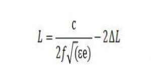
The formula may be used to calculate the trace’s length.
The following factors affect the microstrip width-to-depth ratio:
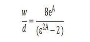
Where w = substrate width, d = trace width, A = effective Area
When PCB Antenna Designing is Complete
After we finish designing the PCB antenna, consulting any internet websites will benefit the production and assembly of PCB boards. The online services will include prototyping, small-batch, and large-volume high-frequency PCB fabrication and assembly. In actuality, several contract manufacturers of complex circuits provide box construction. Viewing several websites and internet videos will aid in a deeper understanding of the idea. Furthermore, we don’t need to be concerned about PCB antenna or other design flaws since the skilled engineers of online companies will review the files before quoting and provide free one-on-one tech assistance!
Conclusion
This article explained all there is to know about PCB antennas, from their definition to how to determine their parameters. The information provided above should make it simpler for you to construct a PCB antenna for your project because they are essential in contemporary applications. For design considerations, keep in mind to consult internet resources offering free tech services and adjust the final design to the particular project.