


 Get A Quote
  (224)366-0290
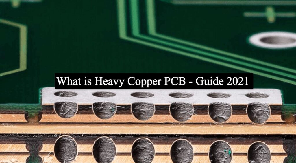
Current industrial requirements are increasingly requiring heavy copper PCB design. These PCBs have found growing usage in the electronics sector, notably in complex switches that must fit into a compact area. This is owing to copper’s strong electrical and thermal conductivity. The end product is a multi-layered or double-sided board with detailed exterior layer(s) and heavy copper layers on the interior layers. As a result, these boards may be found in both power converters and planar transformers.
Heavy Copper PCB Overview
A heavy copper PCB is a board that has a heavy copper circuit. This kind of PCB is subjected to specialized plating and etching techniques such as step plating and differential etching. It is also referred to as a thick copper PCB. After all, copper weights range from 4 oz/ft2 to 20 oz/ft2.
As a result, there is no need to create high-current/high-power circuits and control circuits on separate boards with the thick copper board. In addition, the thick copper plating comes with a simple board design and is highly dense.
What Does Heavy Copper PCB Offer?
Why should you use a heavy copper PCB? Here are a few of the advantages:
Multi-use:
Not every board can endure the weight of the heavy copper PCB without sacrificing board quality or performance. These boards are more likely to be utilized across various devices with variable power and signal levels than regular PCB boards.
Compact size:
Heavy copper boards’ capacity to sustain frequency, high current, high temperature, and recurrent thermal cycles is attributable to many layers’ stocking attributable to many layers’ stacking onto a single layer. This decreases the board’s total size and weight, enabling tiny, high-performance circuits to be used.
Resistant to thermal degradation:
High-frequency boards create a lot of heat, which the fan cooling system cannot effectively disperse. This heat damages the board’s fragile soldered joints, lowering performance and finally destroying it. Due to their increased conductivity, heavy copper PCB boards will create less heat and be away from any external heat at a much faster pace.
Improve Load Sharing:
Instead of generating multiple duplicate and parallel layers, heavy copper can be combined with copper vias. This lowers the load-sharing difficulties associated with numerous parallel levels.
The board’s structural advantage:
A multi-layered heavy copper PCB provides increased mechanical strength because of the stacking of layers and the plated-through holes.
How is Heavy Copper PCB Fabricated?
Plating or etching is commonly utilized in the production of extreme copper PCBs. The primary goal is to increase the copper thickness of sidewalls and plated holes. However, normal etching processes result in unevenly etched margins and edge lines. Therefore, specific etching and plating processes are required to achieve the additional thickness of copper on heavy copper PCBs.
Heavy copper PCBs are electroplated throughout the PCB manufacturing process. This will assist in thickening the PTH barriers on the PCB. As a result, the layer count is reduced, and the impedance distribution is narrowed with this method. However, when PCBs are driven to several cycles throughout the manufacturing process, the plated holes might become fragile.
Methods for Fabricating Heavy PCBs
Blue Bar Method: The Blue Bar Method is used to create automobile PCBs. It entails inserting thick copper bars onto PCBs to transmit the additional current. Because just a few lines are needed to carry more significant current in high-power circuits. This approach saves both time and money by reducing the weight of the PCB. On the other hand, fabricators of multi-layer PCBs must pay close attention to the copper fill level between inner layers in order to prevent additional delamination.
Embedded Copper Method: Using this approach, a thick copper PCB with a heavy copper and flat surface incorporated within the prepreg resin is created. The resin thickness determines the thickness of the heavy copper that must be used.
Difference between a Thick Copper PCB and Standard PCB
The thickness of the copper deposition on the board is the significant difference between regular PCB and thick copper PCB.
The copper layer on a standard PCB weighs one ounce or 35 micrometers, but the copper layer on a thick copper PCB weighs four ounces or 140 micrometers.
Standard PCB cannot conduct large current values; however, extreme copper PCB can perform significant current levels.
Furthermore, standard PCBs do not sustain mechanical stress to enhance heat conductivity.
On the other hand, thick copper PCBs are recognized for enhancing heat conductivity while preserving mechanical stress.
Heavy Copper PCB Capabilities
When employing heavy copper PCB for various applications, it’s vital to evaluate its capabilities. Based on its specifications, this sort of PCB is more expensive to build.
Below mentioned capabilities should be available on a heavy copper PCB:
- A maximum board size of 457mm x 610mm and a minimum board size of 6mm x 6mm is required.
- Copper thickness per square foot is more than 3oz.
- Green, black, blue, red, white, purple, or yellow solder masks are recommended.
- The color of the silkscreen is either white, yellow, or black.
- A board with a thickness of 0.6mm to 6mm
- The maximum copper weight for the exterior layer should be 15 ounces.
- Immersion Gold, HASL, and OSP should be used for surface finishing.
- The final thickness ranges from 0.020 to 0.275 inches.
Applications of Heavy Copper PCB
Heavy copper is widely used in printed circuit boards with high energy (or high current), such as power electronic devices and power supply systems. These PCBs are most observed in the following industries:
Choosing the Right Heavy Copper PCB Manufacturers
When looking for heavy copper PCB manufacturers, there are a few factors to keep in mind:
- Industry Expertise and Capabilities
- On-time Delivery
- Product Quality / Certifications
- Price
Winding Up
Copper PCBs are in high demand due to their consistent performance and excellent thermal control. However, today’s circuits are designed to carry large currents, resulting in a lot of heat. Heavy copper printed circuit boards, on the other hand, will aid in the effective dissipation of heat generated, assuring the circuit’s optimal functioning.