Castellated Holes PCB Guide
What are Castellated Holes on a PCB?
With the development of electronic goods, high density, multi-function, and miniaturization have increased. The boards’ geometric index is increasing day by day, while the size of the PCBs keeps shrinking. Therefore, the soldering process needs an update, as well. Soldering the round hole to the motherboard with soldering flux will result in cold solder. It will cause the motherboard and the daughterboard to have an inferior electrical connection. Mostly due to the largeness of the hole. And as a consequence, the electronic product will not work correctly. So the demand for plated half holes is increasing with each passing day.
[wpi_designer_button twin_id=2164]
What is Castellated Hole (Plated Half Hole PCB)

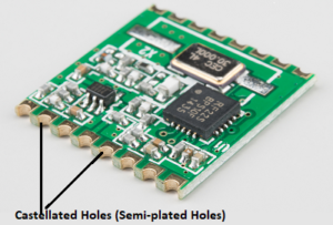
Castellated holes are indentations created on the edges of a PCB board. They are also called castellations. These holes are in the form of semi-plated holes. These holes help in the mounting of one PCB board on top of another. It makes the assembly process much more convenient. However, based on the application, these holes may take the form of a portion of a broken circle. These castellations help provide proper alignment between the two boards. Thus, it helps the appropriate soldering of boards. The castellated holes assist the mounting process, namely board-to-board soldering. You can use castellations in several PCB modules, be it a Wi-Fi module or a Bluetooth module. These modules can be mounted together while soldering, though they are independent parts. These castellated holes connect two PCBs directly. But still, the whole system is noticeably thin, unlike a connection using multi-pin connectors. Through-Hole Technology and Surface Mount technology are among the most commonly used technologies during PCB assembly processes. Board-to-board soldering is also ordinary whenever there is a need to mount two PCB boards together. Castellated holes create a link between the board and the module.
PCB manufacturing process for castellation holes
PCB manufacturing process for plated half holes consists of the following steps.
- Drilling
- Plated hole is ensured
- Panel plating is performed
- Then, Image transfer is done
- Pattern plating is carried out
- Striping
- Then Etching is ensured
- Solder masking is done
- Surface coating happens
- Plated half holes are implemented
However, there are two criteria while stacking one PCB on top of another PCB, using plated half holes.
- The PCB boards ought to have electrical contact. Having only a physical connection is not enough. So make sure that the two boards are connected electrically.
- The boards need to have zero spacing between them. If the boards have even a tiny space between them, the two boards’ soldering will not complete correctly.
Plated half holes are very economical as a technique. It can efficiently transform the circuit board into a type of sub-assembly that is surface mounted. The boards are concave and plated. So they help provide a better landing for soldering. These plated half holes are on the sides of the PCB board. PCB boards using this method will only mount together if there is no space between the two boards. If moisture and dust can gather between the boards, they would not fit.
[wpi_designer_button twin_id=2164]
Why do we use Castellated holes?
The castellated holes reside on the edges of a PCB board. They can replicate many parts of a PCB circuit. Suppose we have a circuit that includes a filter or an inverter. We can mass produce these tiny sub-circuits. Then we can solder them on the main PCB board, containing the other parts of the circuit. In this way, the castellated holes replicate that particular part of the main PCB board. We can use castellations in the following ways:
- Castellated PCBs can act as breakout boards for a particular area of a larger PCB.
- Using these castellated holes, we can change the pin layout of the component as we desire.
- We can mount PCBs with castellations on top of one another with ease.
- Castellated holes combine two PCB boards and validate the joint quality of the soldering.
- Using this method, we can create integrated modules on a single PCB. These modules can help further into another assembly process.
- Breakout boards or tiny modules like Wi-Fi modules make use of this method frequently.
- Castellated holes can also produce wireless PCB to PCB links.
Castellated Holes Design with Images
The castellated holes or castellations make use of a normal via the process. This process includes drilling as well as copper plating. Apart from usual via PCB, there is microtia PCB. Microvia is just a miniature version of a normal via. Microvias typically have a diameter of fewer than 150 microns. These small holes can be created using lasers or in a mechanical way. However, the former acquires a more favorable PCB manufacturing position than the latter for its convenience and continuous improvement. Also, the output in the microvia process is of much higher quality than the normal via. But you are free to choose whatever via process you like according to your needs. Once created, these holes appear like half circles upon the boundaries of the PCB board. This particular shape of theirs is wholly due to their making process. These castellations are cut across so that they create a half hole or partial hole. This partial hole or half hole helps form an opening on the edges of the board. There are several ways of creating castellated holes:
Half holes

Holes featuring smaller cut-in-half holes

Holes featuring smaller lead-in-holes to ensure post-processing (in case of connector applications)

Suggested Specification for Castellated Holes
If you want to use castellated holes for PCB soldering, there are some design attributes. You need to follow these attributes without failing to execute it properly. Below is a list of recommended specifications for castellated holes:
Size: To make your castellated holes PCB mount correctly, select the largest possible size you can get.
Diameter and distance: Plated half holes are used in both standard PCBs as well as advanced PCBs. For standard PCBs, the minimum diameter of holes should be 0.6 mm. For advanced PCBs, the diameter of the castellated holes should be smaller. The minimum distance between two castellated holes should be no less than 0.55 mm.
Surface finish: For the PCBs to mount correctly, you need to take care of the finishing of the surface very sincerely. ENIG finish perhaps the best surface finish for PCBs. However, you can choose your preferred type of finish, depending on the boards’ intended application.
Pad design: For pads, it is better if you use the most massive pad available. Using the most extensive possible for each castellation PCB allows them to fit together correctly.
When using castellated holes for soldering, the number of holes always keeps the number of holes on the board as few as possible. Going for an optimum number of castellated holes will make the alignment and assembly process far more comfortable. However, the number of holes should always be in line with the boards’ design. Do not hesitate to increase or decrease that number as per your needs.
Provided that you follow all the above recommendations, your PCBs are bound to mount together correctly. Not only that but also, the assembly process will be much easier and more convenient.
Applications of plated half holes
The use of castellated holes on PCBs is most common in the following industries.
- Telecommunication
- Computer application
- Industrial control
- Power
- Automobile
- High-end consumer electronics
[wpi_designer_button twin_id=2164]
Call to Action
If you have any doubts regarding the usage of castellated holes on a PCB, feel free to contact us. We are happily here to help you.

