How to Build PCB Kits
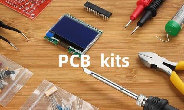
Building your own PCB kits can be a very rewarding experience. Not only will you end up with a functional electronic device, but you’ll also gain valuable skills in soldering, circuit assembly, and troubleshooting. In this article, we will guide you through building a PCB kit from start to finish. Choosing the Right Kit…
What is a Kelvin connection PCB?
Kelvin Connection PCB A particular printed circuit board layout utilized for precise resistance calculations is called a Kelvin connection PCB, also known as a Kelvin detecting or measuring PCB. A Kelvin connection method divides the voltage-sensing and current-carrying pathways to reduce lead impacts and friction resistance. Through employing this technique, mistakes…
What is Numpad PCB
A Numpad PCB is a unique type of pcb used in keyboards and an independent numeric keypad. Its design primarily supports a numerical keypad consisting of numerals, mathematical function buttons, and extra functionality keys. Supporting the electric links between the keyboard’s microcontroller and the keys, the PCB acts like the…
What is PCB Contact?
The conductive spots or connections upon the PCB (printed circuit board) used for attaching or connecting electrical parts are called PCB contacts. These contact points provide the connection that allows for electrical interaction among regions and the printed circuit board. These can be pads, tracks, channels, or other components that provide…
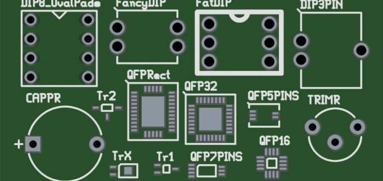
Things to know about PCB footprints
PCB Footprints A PCB’s physical arrangement or measurements are assigned to a particular electrical element as PCB footprints. The dimensions, form, and placement of any pads and solder connections required to attach the part to the circuit board are all shown within these footprints. Throughout the stage of assembly, the footprints…
What is Keyboard PCB Tester?
Keyboard PCB Tester An instrument designed specifically to examine and confirm the keyboard’s PCB (printed circuit board) operation is referred to as a keyboard PCB tester. To evaluate the PCB’s general functioning, switch efficiency, and electrical links, it acts as a tool for diagnosis. By delivering impulses to the circuits to…
How to choose your PCB Dielectric Material
Choosing the right PCB dielectric material is crucial for the performance and reliability of your printed circuit board (PCB). The dielectric layer, which separates the copper traces, affects electrical properties like insulation resistance, breakdown voltage, and loss factor. It also impacts thermal management, structural integrity, and manufacturability. This guide will…
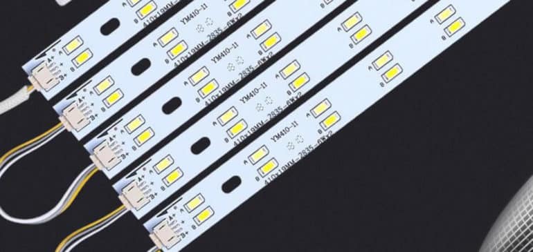
Things to know about flexible LED strip substrates
LED lighting strips, sometimes called LED PCB strips or LED tape, are made from an agile printed circuit board with attached light-emitting diodes (LEDs) organized straight. These light strips give adaptable and energy-effective lighting options by providing illumination for various purposes. LED PCB strips are available in various measurements, shades, and intensities for ambient…
What is PCB Acid Trap?
PCB Acid Trap A PCB acid trap is a layout element utilized on printed circuit boards that keeps etching solvents out of tight places and nooks when the circuit board is being etched. The traps use particular geometrical designs or rounded ends within the printed circuit board structure. They lessen the possibility…
How to Choose the Right PCB Resistor
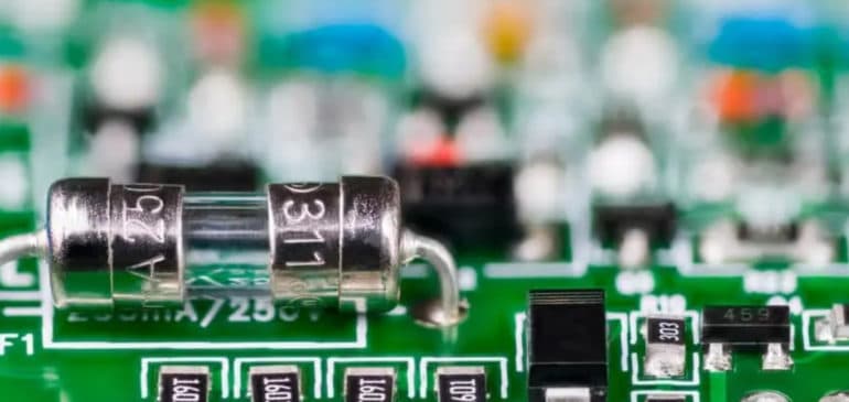
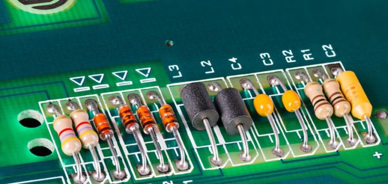
An electronic element called a PCB resistor is utilized in circuits to control the amount of electrical charge that flows through a circuit. They aid in controlling the current and voltage of the circuits and are placed directly into PCBs. Several types of resistors exist, including networks, chip resistors, and surface-mount resistors…

