PCB Breakaway Tabs: Reduce Remnant Materials and Improve Strength
The size of printed circuit boards is becoming smaller and smaller in one or both directions. However, a problem with this cinching is that the raw PCB supplier and the contract manufacturer manage the parts on specific equipment. Mechanisms like routing, electrical testing, and packaging further add cost to the production. Moreover, fallout is also an issue that makes recovery nearly impossible.
However, adding multiple parts to a frame or an array using tabs to hold the single prices in place can be a solution for several years to process printed circuit boards (PCBs). However, it is not the perfect solution as some issues are bound to arise. Join us as we explore the different types of PCB breakaway tabs and how to minimize the problems arising after breaking the individual parts of the component.
How to Palletize Circuit Board and Why?
Palletization was introduced in manufacturing for several reasons. First, it becomes very arduous and challenging to manage smaller printed circuit boards through the manufacturing and assembly processes. ‘Smaller’ means anything less than 3 inches in any direction or both. The smaller the parts, the more complex production becomes in certain areas.
For instance, the standard for the raw card manufactured in a master form is 18 inches x 24 inches. For the components that are singles (1 up) and 2 inches x 2 inches in size, it is possible to process 70 individual pieces on a master. However, when you snip the PCB in half to 1-inch x 1-inch size, you get 280 parts per master, which can be a lot of parts.
But you must be wondering why it is so difficult. For starters, the routine process is very time-consuming. When the router dissects the shape of the PCB, there is also a vacuum removing the dust and debris from the surface. When the PCB is wholly routed, it is possible to vacuum up the smaller parts. Testing is more difficult for such tiny parts, as well, thereby making it compulsory to test these parts in the mind. Lastly, there needs to be more when additions like UL, data code, and serialization are combined.
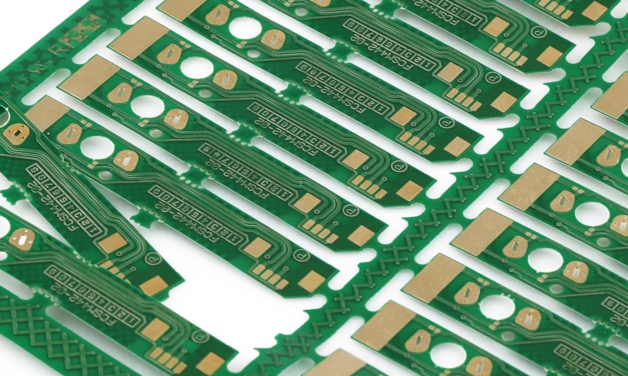
For these reasons, PCB manufacturers or contract manufacturers introduced pallets or arrays. Smaller parts held by tabs are more manageable for production and assembly houses. Of course, there are more wasted materials, but less handling and scraping and a more convenient process result.
Tabs – A Beginner’s Guide
For ease of breaking and removal from the array, the tab part is 0.100 inches to 0.150 inches broad and features non-plated holes, or mouse bites. Based on the design of the tab, the holes may be of different sizes. There is a wide range of breakaway holes used for different reasons.
- Off-board Edge implies that the PCB breakaway tabs have holes entirely off the board edge, with just the radius near the PCB touching the edge. This breakaway design leaves behind more debris that must be manually removed.
- On-board Edge—It enables more perforation holes on the board’s edge. Copper features, lands, and holes on the board determine the holes’ position.
- Combination PCB breakaway tabs – Alternatively known as mouse bites, these breakaway tabs are leveraged to minimize waste material left behind.
Breakaway – A Beginner’s Guide
An item often forgotten is the waste rails or frame around the array. The rails are designed to tolerate handling during the final manufacturing processes and assembly. The array must be strong to prevent breakage and bend. It is also beneficial to secure the components with sturdy rails for support, but this may also make it more difficult to remove the pieces when the item is fully completed.
It is important to remember that an array that is excessively strong and stiff might break and result in expensive repercussions since it takes a lot of effort to remove the boards from the frame. Adding break holes to the rails will aid in disassembly without interfering with the integrity of the parts. When executed appropriately, the parts will easily withstand assembly and be easily removed.
What is a Breakaway Tab PCB?
Simply put, breakaway tabs facilitate assembly. They stimulate the board’s package and enable the designer to determine the precise breakout point. The individual tabs must be centered to avoid protrusion from the side of the PCB. In addition, for further security, four more holes outside the line should be bored.
The unplanted holes can be leveraged to separate tab PCBs; it is essential to be aware of the limitations. For optimal results, the holes must be at least half the width of the PCB. Furthermore, the holes should neither be too large nor too small. Lastly, you need enough breaking tabs to secure the board during PCB construction. Creating a PCB Breakaway Tabs is seamless and hassle-free, but proper and appropriate design is crucial.
Wrapping It Up
So, there we have it—a crisp overview of PCB breakaway tabs and ways to reduce remnant materials and strength. When conjecturing a PCB design and layout, it is crucial to contact your circuit board dealer and discuss the options for array setup with them. You must ensure that the copper is kept 0.010 inches to 0.015 inches away from the edge to allow for proper array setup.
When this arrangement is not possible, breakaway tabs are the best option and are optimal for boards less than 2 inches in either axis. Speak with your contract manufacturer to find out what works best for them. After that, consider component overhangs on larger printed circuit boards to leverage a rail to support the part when applied.

