What Are Gerber Files and How Are They Generated for PCB Design?
Printed Circuit Board (PCB) manufacturing is the foundation of modern electronics, transforming intricate designs into functional hardware. PCBs integrate electrical components, connect circuits, and support the operation of countless devices. However, the transition from design to production requires flawless communication between designers and manufacturers. The Gerber files serves as the industry-standard format, ensuring that every layer of the PCB is accurately represented for fabrication, leaving no room for error.
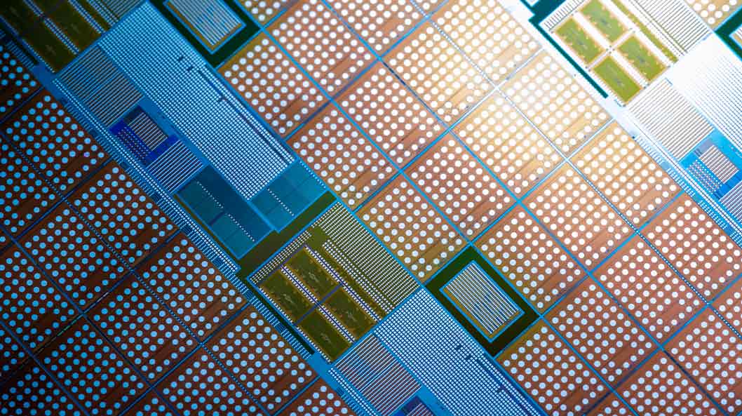
A Gerber file encapsulates precise details of a PCB’s layout, including copper traces, drill hole positions, solder masks, and silkscreen layers. It acts as the blueprint that guides manufacturers in producing a PCB exactly as envisioned. This article explores the technical details of Gerber files, their critical role in PCB design, and the step-by-step process of generating them using advanced Gerber PCB software.
What is a Gerber File?
A Gerber file is a standardized file format used in PCB manufacturing to describe the design’s layout. It includes precise details about copper traces, component placements, drill holes, and layer-specific data. These files are compatible with various Gerber PCB systems and are essential for ensuring that manufacturers can interpret and fabricate the design without ambiguity.
Gerber files are classified into two main formats:
- RS-274-D: The older format, now largely obsolete.
- RS-274X: The extended version, which incorporates embedded aperture definitions and is the industry standard.
Importance of Gerber Files in PCB Design
Gerber files are a critical component of PCB design, serving as the universal standard for conveying design data to manufacturers. These files include detailed layer-by-layer instructions, covering copper traces, solder masks, silkscreen markings, and drill hole information. Their standardized structure ensures that PCB design are accurately interpreted and fabricated without discrepancies, regardless of the complexity of the circuit.
The precision and reliability of Gerber files eliminate ambiguity in the manufacturing process, making them indispensable in modern PCB workflows. They support seamless integration with various Gerber PCB software and fabrication tools, ensuring a smooth transition from digital designs to physical boards.
- Gerber files define copper traces and pads for all PCB layers.
- Drill data specifies via locations and hole diameters with high precision.
- Solder mask layers protect copper traces and prevent shorts.
- Silkscreen files include detailed component labels and markings.
- Standardized formats ensure compatibility with fabrication equipment.
- Manufacturers use Gerber files for accurate layer stacking and alignment.
- Gerber viewers allow designers to verify files and detect errors.
- Layer-specific files ensure clarity and eliminate misinterpretation risks.
- Advanced Gerber PCB software automates error-checking and output generation.
- Complex multilayer PCBs are easily managed using Gerber files.
- Fabrication efficiency is enhanced through standardized data handling.
The Process of Generating Gerber Files
Generating a Gerber files requires specialized Gerber PCB software. The process involves several key steps, typically executed within PCB design tools like Altium Designer, KiCAD, or Eagle. Below is a breakdown of the process:
- Design Your PCB Layout: The first step involves creating the PCB layout using CAD tools. Each layer, from copper traces to silkscreen, is designed digitally.
- Set Up Output Layers: Configure the software to generate separate files for each layer of the PCB. For instance:
a.Copper layers (top and bottom)b.Solder mask layersc.Silkscreen layersd.Drill files - Select the File Format: Ensure that the output format is set to RS-274X for compatibility with modern Gerber circuit board software.
- Generate Gerber Files: Export the design into individual Gerber files. This typically involves selecting “Generate Gerber” from the tool’s export menu.
- Verify the Files: Use a Gerber viewer to inspect the generated files. Tools like GerbView and ViewMate allow you to check for errors before submitting the files for fabrication.
Role of Gerber PCB Software in File Generation
Gerber PCB software plays a pivotal role in the creation and validation of Gerber files, ensuring seamless communication between PCB designers and manufacturers. This software is designed to handle complex PCB layouts, generate precise layer-specific data, and ensure compatibility with manufacturing equipment. The reliability of Gerber files largely depends on the capabilities of the software used during the file generation process.
Modern Gerber PCB software streamlines the process of converting PCB design into production-ready Gerber files by automating intricate tasks. It enables designers to configure settings for each layer of the PCB, including copper, solder mask, silkscreen, and drill files. Software tools like Altium Designer, KiCad, and Eagle provide robust interfaces for managing these configurations, allowing designers to ensure accuracy and consistency in their outputs.
Advanced error-checking features in Gerber PCB software detect design flaws or missing elements before file generation. This includes identifying issues such as overlapping traces, unconnected pads, and incorrect drill sizes. Such pre-emptive checks reduce the likelihood of errors during fabrication, ensuring a more reliable transition from digital design to physical PCB.
Transitioning from Gerber to PCB Manufacturing
The shift from Gerber files to PCB manufacturing is a critical phase in ensuring a design moves from concept to production. Gerber files contain all the essential details required to fabricate a printed circuit board, but this step necessitates careful translation to ensure manufacturing precision. Accuracy in the design and an understanding of production limitations are essential to avoid errors in the final product.
Effective management of this transition requires attention to specific areas such as design verification, material selection, and trace width calculations. These aspects directly impact the quality, functionality, and manufacturability of the PCB, demanding careful optimization throughout the process.
Design Verification
Ensure all Gerber files are complete, error-free, and adhere to the specifications. Conduct rigorous checks to confirm the design meets the manufacturing requirements and avoid potential issues in later stages.
Material Selection
Select appropriate PCB materials that meet both electrical and mechanical performance criteria. This includes the choice of laminate materials, solder mask, and surface finish to ensure durability and reliability.
Layer Stack-up and Trace Width
Define the correct layer stack-up based on design complexity and select trace widths that are compatible with current handling capabilities and manufacturability limits.
Component Placement and Routing
Place components with precision, considering ease of assembly and electrical performance. Optimize routing to minimize interference, while ensuring sufficient clearance for signal integrity.
Prototype Testing
Test prototypes to verify design performance and adjust before committing to full production. Ensure that pre-production testing confirms the design’s manufacturability and meets all quality standards.
Wrapping it up
Transitioning from Gerber files to PCB manufacturing is an exciting yet detailed process that requires precision and a clear understanding of each step. Whether you’re refining your design or finalizing materials, the goal is always to ensure that the final product performs as intended and meets all expectations. With careful planning and attention to every detail, you can make sure your design becomes a functional, high-quality PCB ready for the market.
In the end, this process is all about making your ideas come to life in the most effective way possible. The key is to be thorough, stay informed about manufacturing capabilities, and embrace the learning curve along the way. The more you adapt, the more seamless the transition will be—leading to a successful final product that delivers real-world value.
Want to know more about Gerber files and how important it is in PCB design? – Let’s connect now.