


 Get A Quote
  (224)366-0290
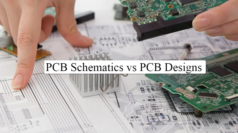
Many users are found to use PCB Schematics and PCB Designs interchangeably. However, these two are not the same. These stand for two different types of representations of a PCB board. So, let’s try finding out how these two differ and what these represent.
What is a PCB?
PCB stands for printed circuit board. It is a bare board that has the design of interconnections among various components imprinted on it. There is another term used commonly called as PCBA or printed circuit board assembly. It differs from PCB in the fact that while PCB is just the design of the circuit, the PCBA is design plus the components fixed on to it. The cost of PCB assembly is determined by the schematic first and then by design.
PCB material, component quality, circuit work, etc. together differentiate one PCB from another. PCB is also known as printed wiring board or PWB.
To understand the utility of various PCBs, the very first step is to design its schematics. The schematics are like a line diagram. Based on the PCB or circuit board schematics, the PCB designs are developed. So, let’s understand how both differ and contribute to the PCB development process.
PCB Schematics vs PCB Designs
A PCB comprises of various electrical components. The interaction and connection flow among these components are represented in the form of PCB schematics. The schematic show the use and utility of various electrical components of both the active and passive nature. The components usually comprise capacitors, integrated circuits, resistors, and so on. These components, when arranged in a readable format, constitute the PCB schematics. With the help of this schematic, the visualizers can find connectivity among different components. Here is the diagram of the PCB schematics:

Diagram of the PCB schematic
PCB schematics is designed to simplify the understanding of the components’ arrangement on the board. It offers a more straightforward and easily readable representation of the electrical circuits arranged.
The diagram of a PCB designs is shown below. It can be referred to as the modular presentation of all the components appearing in the PCB schematics.

Thus, the difference between the two is quite crisp and clear. We can easily say that the PCB development process flows from schematic to PCB designs.
PCB Schematic Elements with Image
PCB Schematic Elements include the electrical and electronic components of both active and passive nature.
Active components are comprised of:
- Different styles of transistors – JEETs, MOSFETs, FETs, etc.
- Generators such as DC generators and alternators
- Diodes
- Current and voltage sources, etc.
Passive components include:
- Transformers
- Inductors
- Capacitors
- Resistors

Simple Presentation of the schematic elements
Displayed above is the diagram that is a simple presentation of the schematic elements. It shows how different elements are arranged to control the flow of electricity in various parts of the circuit.
PCB Designs Elements
The most commonly used PCB Designs is the one derived from the use of SMT or Surface Mount Technology. The PCB design elements mainly comprise of:
- PCB pattern,
- Size, location hole,
- Panel methods,
- MARK,
- clamping edge, etc.
PCB pattern
PCB pattern is nothing but the arrangement of components that enables smoother and controlled pathway transmissions among them. The pattern also enables seamless carrying out of processes that are aligned in a sequence. In an automated process, the sequence comprises steps such as printing, mounting of chips, soldering. Finally, this is converted into a finished board using an unloader.
PCB can be designed in different patterns. One such patterns types is a rectangular pattern.
PCB location hole and size
Usually, the PCB location hole method in a typical SMT style is of two types – only edge location and location hole with edge location. Some makers employ specialized hole methods like Fiducial Mark.
The size has to be optimal when it comes to attaining an efficient PCB design. Too small a PCB design can make configuration of components different and too big adds to the cost and also needs specific device design, which may not be feasible always.
Panel methods
Using the correct panel method is important for attaining efficient manufacturing and responsive PCB design. To achieve this efficiency, multiple PCBs of small size and differently compatible shapes are combined. This arrangement is called a panel. The PCBs that have double sides, the top, and bottom sides, are made into a single panel to achieve a stencil-like design. The panels are connected using any of the process options, such as the V groove and stamp hole methods.
MARK
It is the most crucial PCB design element. MARK is identified based on shape, size, and surface.
- Shape: solid circle, hollow circle, rectangle, rhombus, oval, etc. are some of the choices
- Size: Size can vary from 0.5mm to 3mm
- Surface: optimal thickness with exceptional reflector effect
Note: A background zone should be well-defined around the MARK and other pads. It should not comprise of silkscreen or solder mask.
Clamping edge
Types of clamping edge achieved by the PCB designers are – pathway clamping edge, open space supplemented, and crack edge.
Thus, all these design elements are to be taken into account while trying to achieve a feasible and fully functional PCB design. There are different variations available in each design element. The designer has to pick the relevant characteristics of each of these elements into account for making the PCB design fully compatible with the needs of the development process of the device.
Conclusion
Looking at the explanations of PCB schematics and PCB designs above, one can safely infer that both the terms are different and quite distinct. Both of these have an essential part to play in the PCB development process. While the clarity of pathway flow is essential for achieving the PCB schematics, the PCB designs works out better when its elements are selected while conforming to the device’s requirements.
An excellent schematic to PCB layout process is the one that offers crystal clear understanding of the components and their relationships; an excellent PCB designs is one that contributes to achieving good product quality, aesthetically as well as functionally.