How PCB fabrication quality directly affects solder joint reliability
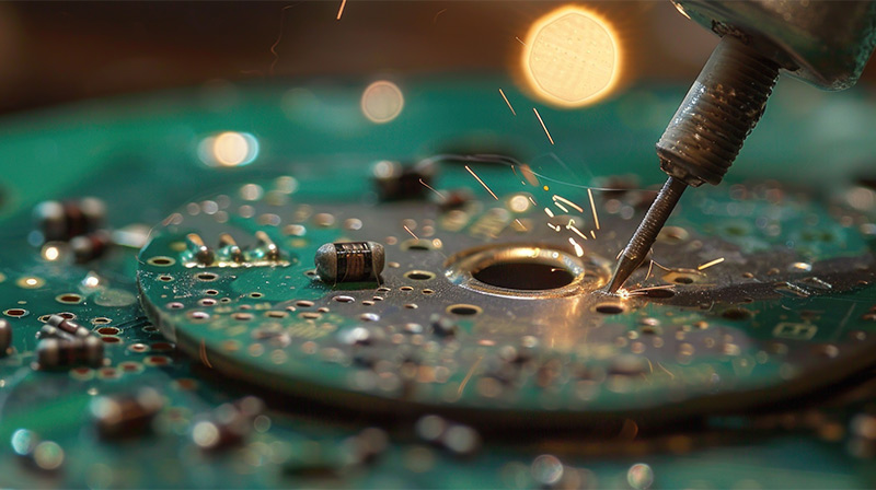
Solder joint reliability is one of the most decisive factors in the long-term performance of electronic products. While assembly processes often receive most of the attention, many solder failures originate much earlier during PCB fabrication. When the base board itself carries material or structural inconsistencies, even the best assembly practices struggle to deliver stable results.
In high-volume and high-reliability applications, solder joints must survive repeated thermal cycles, vibration, electrical stress, and extended operating hours. This makes PCB manufacturing quality a foundational requirement rather than a secondary concern. Circuit board manufacturing that lacks consistency introduces hidden risks that surface only after deployment, where corrective action becomes expensive and disruptive.
In this article, we explain why PCB fabrication quality has a direct impact on solder joint reliability, what fabrication factors matter most, and how choosing the right printed circuit board manufacturers helps reduce long-term failure risks.
Why PCB fabrication quality matters for solder joint reliability
PCB fabrication quality sets the physical and material foundation on which every solder joint is formed during PCB assembly. Factors such as copper thickness, surface finish behavior, laminate bonding strength, and dimensional stability are all defined during PCB manufacturing, long before components are placed. Any variation at this stage directly affects how solder melts, wets, and solidifies during reflow. In circuit board manufacturing, these fabrication parameters also influence how joints respond to thermal cycling, vibration, and electrical load over time.
When PCB fabrication quality is inconsistent, solder joints may appear acceptable initially but degrade under real operating conditions. This is why printed circuit board manufacturers treat fabrication control as a key driver of long-term solder joint reliability rather than just a production step.
- PCB fabrication quality controls solder wetting behavior by defining copper surface condition and surface finish uniformity during PCB manufacturing.
- Variations introduced during circuit board manufacturing alter heat absorption at the pad level, causing uneven solder melting and internal stress formation.
- Poor surface finish control during PCB fabrication reduces solder adhesion strength, leading to joints that fail under repeated thermal cycling.
- Inaccurate solder mask registration from PCB manufacturing allows solder to spread beyond pad boundaries, weakening joint geometry and stability.
- Weak laminate bonding in circuit board manufacturing lowers copper peel strength and increases the likelihood of pad lifting during reflow or rework.
- Board warpage originating in PCB fabrication prevents uniform component contact, resulting in partial wetting and mechanically weak solder joints.
- Inconsistent via plating quality during PCB manufacturing changes stress distribution, accelerating solder joint fatigue in multilayer designs.
Key PCB fabrication factors that influence solder joint reliability
PCB fabrication controls multiple physical and chemical characteristics that shape how solder joints behave during assembly and throughout the product lifecycle.
Copper thickness consistency
Copper thickness affects both heat transfer and mechanical strength at the pad level. During PCB fabrication, uneven copper plating alters how heat flows through the pad during reflow, which changes solder wetting behavior.
Thin copper reduces pad strength and increases the risk of pad lifting during thermal cycling or rework. Excessively thick or uneven copper increases thermal mass, slowing solder flow, and creating stress concentration points. Circuit board manufacturing processes that maintain consistent copper thickness support stable joint formation and longer fatigue life.
Surface finish quality and uniformity
Surface finish is the direct interface between solder and copper, making it a critical factor for joint reliability. In PCB manufacturing, variation in finish thickness or contamination weakens solder wetting and intermetallic bonding.
Poor surface finish control often leads to dull joints, incomplete wetting, or early cracking under thermal stress. Printed circuit board manufacturers that maintain stable finish chemistry and uniform deposition ensure predictable solder behavior across all pads during assembly.
Solder mask alignment and pad definition
Solder mask accuracy determines how solder paste is confined during reflow. Misaligned or inconsistent solder mask openings expose excess copper and allow solder to spread beyond intended boundaries.
This affects joint shape and increases bridging risk in dense layouts. During PCB fabrication, solder mask errors often originate from panel distortion or curing inconsistency. Proper pad definition supports controlled solder volume and stronger mechanical joints.
- Accurate mask registration maintains consistent solder joint geometry
- Uniform mask thickness limits uncontrolled solder spread
- Clean mask edges support repeatable wetting behavior
- Stable curing prevents mask cracking during thermal exposure
Laminate quality and copper adhesion strength
The laminate material beneath copper pads defines how well those pads survive thermal stress. Low-quality laminates or weak bonding reduce peel strength, making pads vulnerable to lifting during assembly or later repairs.
In circuit board manufacturing, poor laminate adhesion may not be visible during inspection but becomes evident after repeated heating cycles. PCB fabrication processes that ensure strong copper-to-laminate bonding improve joint durability and reduce rework-related damage.
Board flatness and dimensional stability
PCB flatness directly affects component contact during placement and soldering. Warped boards prevent uniform pressure between pads and lead, resulting in uneven solder thickness and partial wetting.
In mass PCB manufacturing, small flatness deviations multiply into large defect volumes. Controlled lamination balance and cooling during fabrication help maintain stable board geometry, supporting consistent solder joint formation.
- Flat boards ensure even solder contact during reflow
- Dimensional stability improves placement accuracy
- Reduced warpage lowers open joint risk
- Consistent geometry supports repeatable assembly results
Via structure and internal bonding quality
Vias influences how thermal and mechanical stress travel through the board. Poor via plating or internal voids weaken structural integrity and increase joint fatigue, especially in power and multilayer designs.
PCB fabrication processes that control via wall thickness and internal bonding help distribute stress evenly across solder joints. This improves reliability under continuous electrical load and temperature variation.
How choosing the right PCB manufacturer improves fabrication quality
- The right PCB manufacturer maintains strict material qualification processes that stabilize laminate quality and copper bonding during PCB fabrication.
- Experienced printed circuit board manufacturers control copper plating thickness and uniformity to support reliable solder joint formation during PCB manufacturing.
- Strong circuit board manufacturing partners invest in advanced solder mask registration systems that improve pad definition and solder volume control.
- Reliable PCB manufacturers enforce surface finish consistency through controlled chemistry, process monitoring, and batch-level validation.
- Established PCB fabrication facilities maintain tight dimensional tolerances that reduce warpage and improve placement accuracy during PCB assembly.
- Quality-focused manufacturers use process traceability to link fabrication parameters with assembly outcomes, enabling faster root-cause correction.
- PCB manufacturers with integrated engineering teams align fabrication tolerances with assembly requirements to reduce defect risk at scale.
- Long-term manufacturing partners continuously improve fabrication stability through data-driven process optimization rather than reactive corrections.
Conclusion
Solder joint reliability is directly shaped by PCB fabrication quality. Factors such as copper consistency, surface finish control, solder mask accuracy, laminate strength, and board flatness define how joints form and how they survive long-term stress. When these fabrication elements are stable, assembly processes become predictable and reliable.
For OEMs and engineering teams, working with experienced printed circuit board manufacturers reduces quality risks at the source. If you are looking to improve solder joint performance and long-term reliability, connect with the experts at Absolute PCB Manufacturers to get fabrication and PCB manufacturing support built for consistent, high-quality results.