


 Get A Quote
  (224)366-0290
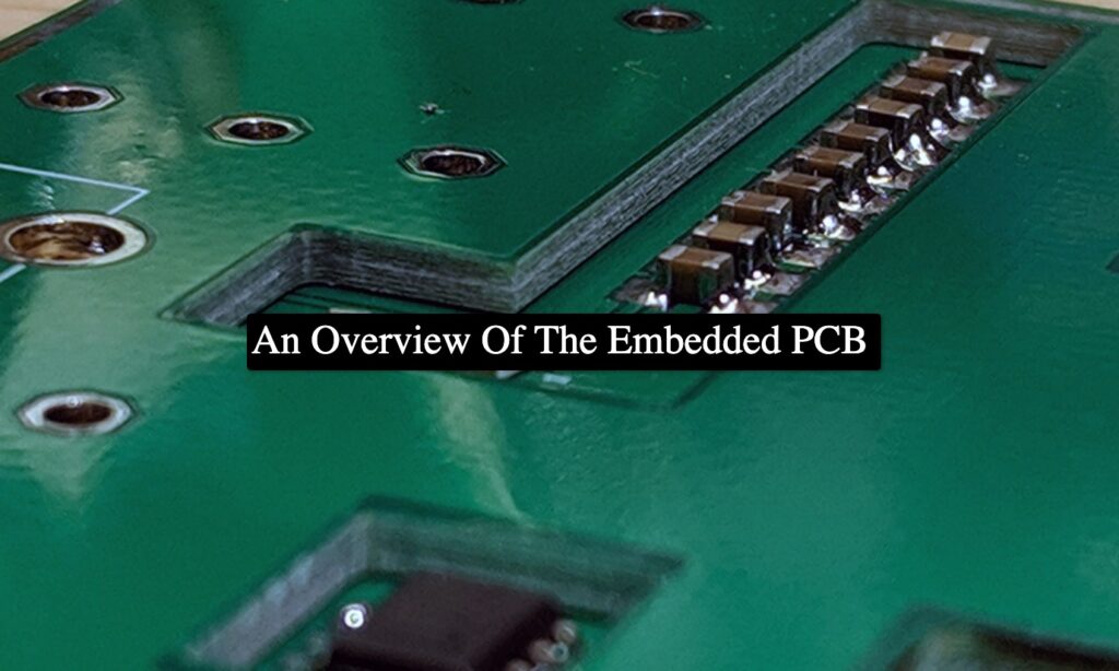
Technological revolutions occur rapidly, and you cannot afford to lag to stay relevant and competitive in this dynamic field. Such has been proved by the trend of Printed Circuit boards, especially in the field of electronic manufacturing, designing, and assembly. If you are a designer of electronic PCBs or want to learn more about embedded PCB, you should read this article to learn about all aspects of the embedded printed circuit board.
About Embedded PCB
Recently, there has been a growing demand for electro-medical, wearable, and mobile devices, which has permeated every part of the world. Hence, it has also increased the demand for embedded PCBs, but the progressive size reduction of these types of PCBs is reduced drastically. However, with the demand for new attributes like the HD display, and wireless connectivity for smartphones, the demand and increased pressure for having better component density on the reducing size also exist, which is an abrupt and unexpected challenge embedded PCB wants to solve.
So, what is the implication of an embedded PCB? The embedded PCB infers the printed circuit board, which has embedded components that enhance efficiency and provide top-notched performance. It is made with embedding technology, which is instrumental in reducing transmission losses and decreasing the interconnection path among the components. This plays an integral role in the size reduction of the PCB, IP protection, function integration, and increased reliability.
The Assembly Process For Component Embedded Printed Circuit Board
One primary feature of the embedded PCB design is the components integrated into the printed circuit boards. The embedding technology consists of mounting and has two types: Thru-hole and solder pad mounting methods.
Thru-Hole Mounting Method: It entails the chip and bare mounting processes, although the subsequent options vary from the solder pad mounting process. The bare mounting has the plated thru-hole or the conductive adhesives. The route for the chip mounting has similar options, which are the conductive adhesive thru-hole and plated thru-hole options.
Solder Pad Mounting Method: This method uses the bare dire and chip mounting procedure. Initially, the bare method consists of the wire mounting process called flip-flop mounting. Choosing which to go through when embedding the components on your printed circuit board would be best. Secondly, having a printed circuit board in the embedded system also entails the chip mounting process from which you can decide whether you want to adopt conductive resin and wave soldering.
Please remember that the mounting method in the embedded PCB with pads needs components assembly on the formed electrodes other than developing the electric connections. The insulating resin’s application is then carried out to bury and fill the components and electrodes.
Assembly Process For Embedded Components In PCB
Before moving to the Embedded PCB design and assembly process, it is necessary to note the following down of the assembly process. Initially, it is essential to use the die bonding for the bare die components and the mold packaging for the pad components. The CCCC, WLCSP, ESC, Ultrasonic Wave Bonding, and conductive resin can also be used. However, you should choose wave solder and conductive resin when using the AD mounting.
The better comprehend the assembly process for the components of the embedded PCB. Considering one mounting process and looking at it more deeply becomes crucial.
Assembly Process For Embedded Tech With Pads
- The first is to do prudent research on the design and technological process, especially for the AD tech possibility, and the SMDs will also be embedded in the PCBs cavity.
- The next integral step is trace designing.
- Assembly embedded in the components cavity.
- The manufacturing process of the embedded PCB process is the subsequent step and has the whole process. Dealing with double-layer PCB begins with the double-layer substrate’s fabrication before adding layering of the soldering paste. It will then continue with the IC assembly e and the waves soldering right before the filling of the insulation and mid-stack ups. Lastly, the process will be completed with top coating, hot pressing, and stack-ups.
- One primary challenge with the embedded PCB is the components’ assembly in the cavity. You will be facing the chance of failing the application of old solder paste printing tech in the planar pattern. On the other hand, the seamless exhaustion of the gas within the cavity may fail during wave soldering. Consequently, it can lead to a higher voltage of solder. Adopting the printing workflow of solder paste, vacuum wave soldering, and mounting is crucial to prevent this from occurring when using solder printing and vacuum wave techniques. Once done, spray coating, plugging, and cleaning transpire before completing the process.
Printed Circuit Board Designs For Embedded Systems
The embedded PCB design is critical for the manufacturing process of printed wiring boards. Due to this, learning a few things about PCB designs for embedded systems is necessary.
- Size Of PCB: Size usually is the primary obstacle in PCB design. Hence, the PCB layout and size need every party, from engineers to designers, and agree on all parts. However, both parties should agree not to exceed the minimum size limit. It cannot become significantly small since you will have to ensure that the appropriate positioning of the component happens and that it does not overheat. The embedded system comes with passive components and needs SMD tech, which is mandatory. It decreases the footprint and distance between the components, which results in a compact PCB layout. Another aspect entails the PCB routing’s optimization. Moreover, if there is space, increasing the trace placement and layer numbers is necessary.
- Thermal Management: heat production occurs on the tracing when a high-intensity current flows. Hence, it is necessary to enhance the thermal dissipation to keep the small size of the PCB. You can do it using one of the two methods, such as increasing the trace thickness, developing the printed circuit board regions, and getting the needed heat dissipation. When doing this, make sure that you are following the IPC2221A standards. It involves using copper planes with a thickness of about 10 ounces, though the value will be increased. Moreover, the hot spots creation will be eliminated by maintaining the maximum temperature of 170 degrees Celcius. You can also use the thermal imager to find such hotspots.
- Components Placement: the placement of the components usually reflects and follows the designing rules of the PCB. The rules involve precise alignment, which follows the simple assembly and the efficient soldering process. Moreover, proper separation should be enforced between analog and digital devices. Also, try to avoid placing heavier components near the PCB edge since the board can be bent.
- Embedded Components: Most embedded systems have small footprints with elevated device density to simplify the design and assembly phases. Consequently, the inductors, resistors, and capacitors should be embedded inside the PCB. It will reduce the tracing length and the soldering point numbers. With this, you will get better electrical performance other than circuit reliability. The resistors, inductors, and capacitors will be placed on the inner layer through the etching process during the manufacturing of the PCBs. Subsequently, for the embedded PCB, these components are incorporated during the lamination process.
Conclusion
The embedded PCB has become essential for all electrical devices due to its diverse specifications needed by the users. Hence, if you want the universal acceptance and success of the PCB design, you should opt for the embedded PCB.